Electro-optical device, electronic apparatus, and contact detection method

a technology of optical devices and electronic devices, applied in the direction of instruments, electric digital data processing, computing, etc., can solve problems such as difficulty in obtaining accurate contact judgment, and achieve the effect of high judgment accuracy

Inactive Publication Date: 2009-11-19
JAPAN DISPLAY WEST
View PDF12 Cites 57 Cited by
  • Summary
  • Abstract
  • Description
  • Claims
  • Application Information

AI Technical Summary

Benefits of technology

[0006]An advantage of some aspects of the invention is provide an electro-optical device, an electronic apparatus, and a cont

Problems solved by technology

Therefore, it is difficult to obtain an accurate contact judgment resu

Method used


Image

  • Electro-optical device, electronic apparatus, and contact detection method
  • Electro-optical device, electronic apparatus, and contact detection method
  • Electro-optical device, electronic apparatus, and contact detection method

Examples


first embodiment

A: First Embodiment

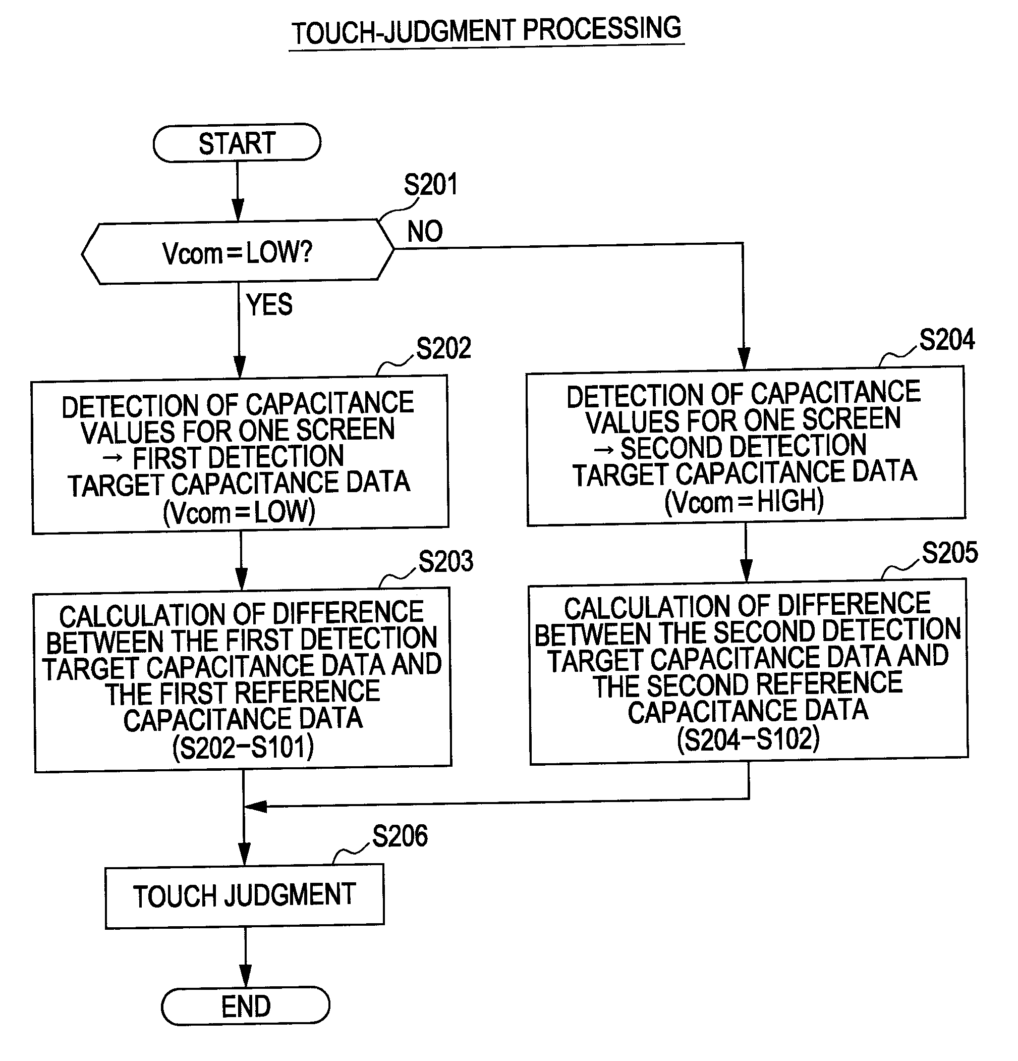
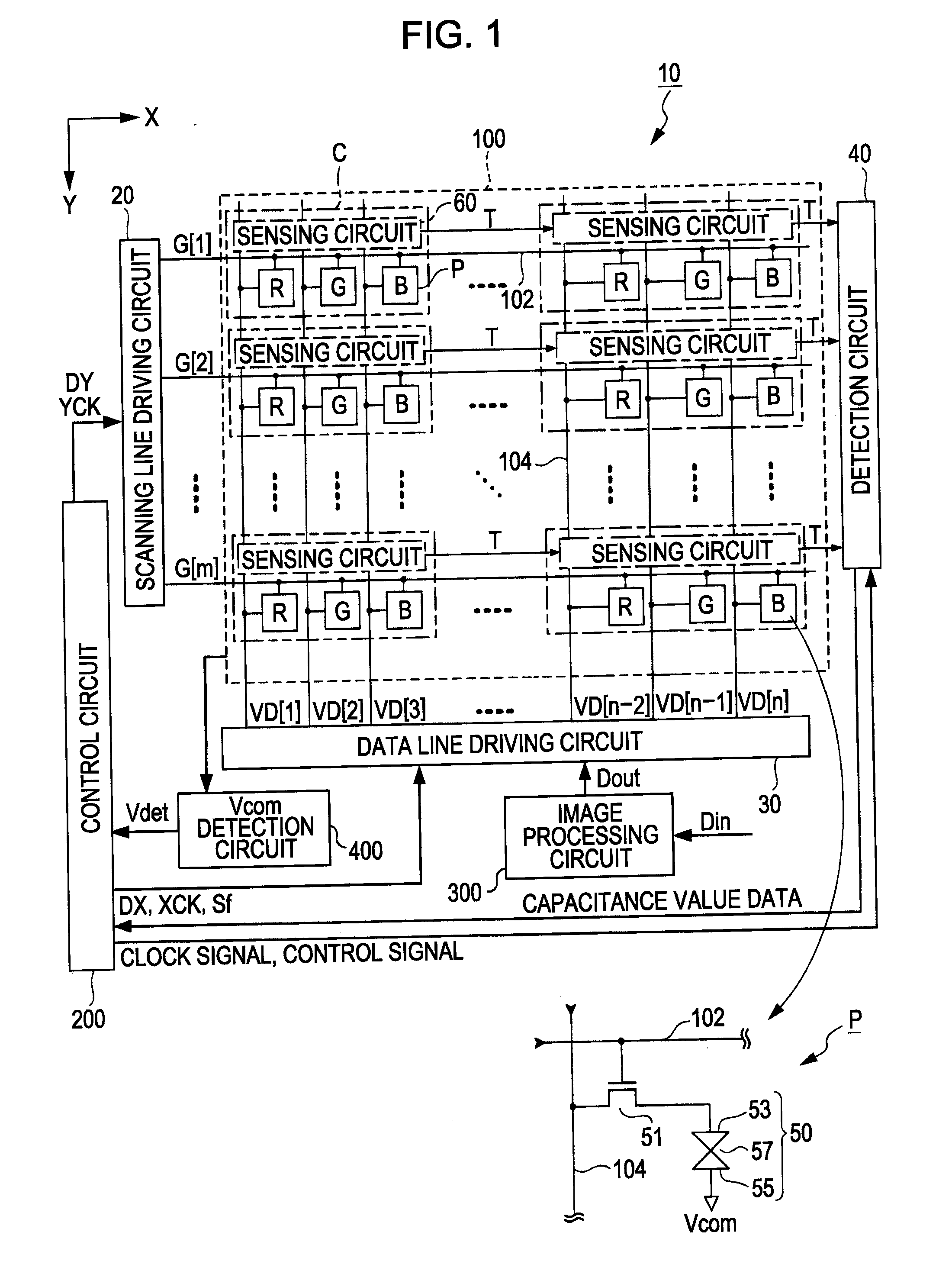
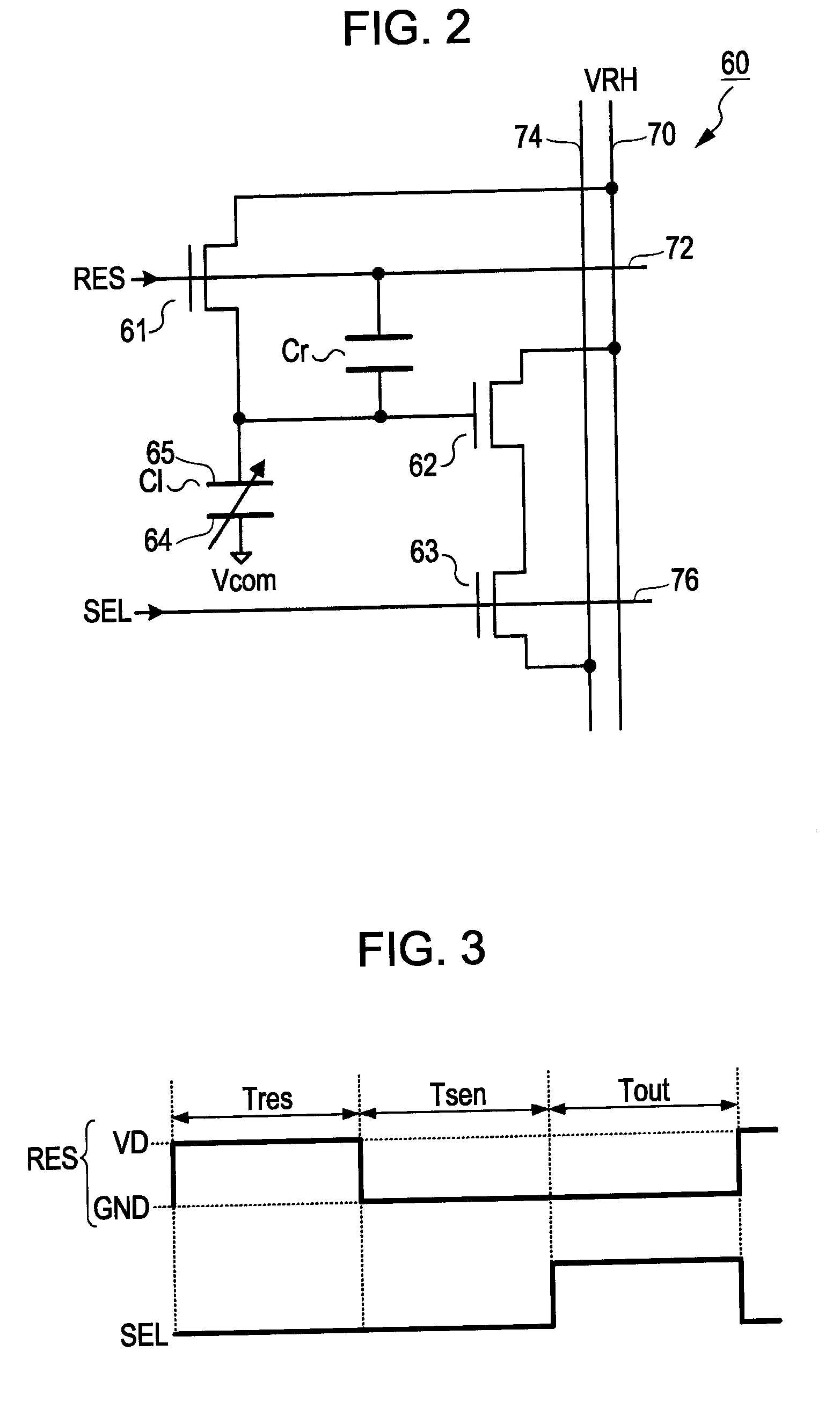
[0046]FIG. 1 is a block diagram that schematically illustrates an example of the configuration of an electro-optical device 10 according to a first embodiment of the invention. As illustrated therein, the electro-optical device 10 is provided with a pixel area 100, a scanning line driving circuit 20, a data line driving circuit 30, a detection circuit 40, a control circuit 200, an image processing circuit 300, and a Vcom detection circuit 400. The pixel area 100 has a plurality of lines formed thereon. Specifically, “m” scanning lines 102 are arrayed in parallel with one another in such a manner that each thereof extends in the X direction in the pixel area 100, where “m” is a natural number that is greater than two, or, at the smallest, equal to two. On the other hand, “n” data lines 104 are arrayed in parallel with one another in such a manner that each thereof extends in the Y direction in the pixel area 100, where “n” is also a natural number that is greater t...

second embodiment

B: Second Embodiment

[0084]Next, with reference to FIG. 15, an electro-optical device according to a second embodiment of the invention is explained below. The basic configuration of an electro-optical device according to the present embodiment of the invention is substantially the same as that of the electro-optical device 10 according to the first embodiment of the invention, which is explained above while referring to FIGS. 1-12. Accordingly, in the following description of this specification, the same reference numerals are consistently used for the same components as those described in the first embodiment of the invention. Note that redundant explanation will not be given for the components of an electro-optical device according to the second embodiment of the invention that are the same as those of the electro-optical device 10 according to the first embodiment of the invention.

[0085]Upon the start of initialization processing illustrated in FIG. 15A, the control circuit 200 c...

third embodiment

C: Third Embodiment

[0090]Next, with reference to FIG. 16, an electro-optical device according to a third embodiment of the invention is explained below. The basic configuration of an electro-optical device according to the present embodiment of the invention is substantially the same as that of the electro-optical device 10 according to the first embodiment of the invention, which is explained above while referring to FIGS. 1-12. Accordingly, in the following description of this specification, the same reference numerals are consistently used for the same components as those described in the first embodiment of the invention. Note that redundant explanation will not be given for the components of an electro-optical device according to the third embodiment of the invention that are the same as those of the electro-optical device 10 according to the first embodiment of the invention.

[0091]Upon the start of initialization processing illustrated in FIG. 16A, as a first step thereof, the...


PUM


Abstract

An electro-optical device includes: a screen on which an image is displayed; a first substrate and a second substrate that are provided opposite to each other; liquid crystal that is sandwiched between the first substrate and the second substrate; an electrostatic capacity detecting unit that outputs a detection signal whose level corresponds to the value of a capacitance that is formed by the liquid crystal, a first electrode, and a second electrode; an image displaying unit that includes the liquid crystal, a third electrode, and a fourth electrode, the image displaying unit controlling the transmission factor of the liquid crystal for displaying an image on the screen; a first memory unit that memorizes the level of the detection signal outputted by the electrostatic capacity detecting unit in a state in which a detection target object is not in contact with the screen as reference data; a second memory unit that memorizes the level of the detection signal outputted by the electrostatic capacity detecting unit in a state in which a judgment is made as to whether the screen is contacted or not as detection target data; a difference data generating unit that generates a difference between the reference data that has been read out of the first memory unit and the detection target data that has been read out of the second memory unit as difference data; and a judging unit that judges whether the detection target object is in contact with the screen or not on the basis of the difference data.

Description

BACKGROUND[0001]1. Technical Field[0002]The present invention relates to an electro-optical device, an electronic apparatus, and a contact detection method for detecting the touching of an object such as a finger, a pen, or the like on a screen.[0003]2. Related Art[0004]A liquid crystal display device that has a touch-screen function is described in JP-T-2007-510949. The related-art liquid crystal display device that is described in JP-T-2007-510949 judges whether a screen is touched or not by detecting a change in the capacitance value of a capacitive element, which is made up of two electrodes that are respectively provided on two substrates arrayed opposite to each other and liquid crystal that is sandwiched between these electrodes.[0005]In the operation of a liquid crystal display device, an alternating voltage is applied to liquid crystal in order to prevent the occurrence of image quality degradation such as a burn-in problem or the like. For example, a data electric potentia...

Claims


Application Information

Patent Timeline
IPC IPC(8): G06F3/044
CPCG06F3/0412G09G3/3648G06F3/044G06F3/0445G06F3/04166G06F3/0443G02F1/13338
Inventor CHINO, TAKETO
Owner JAPAN DISPLAY WEST
Why Eureka
Try Eureka