Display device, method of laying out light emitting elements, and electronic device

a technology of light emitting elements and display devices, applied in semiconductor devices, instruments, computing, etc., can solve the problems of reducing the period of an electrooptic element, reducing the power consumption of the display device, and reducing the difficulty of realizing a large and high-definition display device, so as to achieve excellent display quality and reduce the effect of changing the characteristics of the pixel transistor from color to color due to the effect of leakage light from an adjacent pixel

Inactive Publication Date: 2009-11-26
SONY CORP
View PDF9 Cites 36 Cited by
  • Summary
  • Abstract
  • Description
  • Claims
  • Application Information

AI Technical Summary

Benefits of technology

[0029]According to the present invention, variations in changes in characteristics of the pixel transistor from color to color due to the effect of leakage light from an adjacent pixel can be reduced. Thereby, a white balance can be maintained without depending on an image being displayed, so that a display image of excellent display quality can be obtained.

Problems solved by technology

The organic EL element can be driven by an application voltage of 10 V or lower, and thus consumes low power.
However, while having a simple structure, a simple matrix type display device presents for example a problem of difficulty in realizing a large and high-definition display device because the emission period of an electrooptic element is reduced by an increase in the number of scanning lines (that is, the number of pixels).
As a result, screen uniformity is impaired.

Method used


Image

  • Display device, method of laying out light emitting elements, and electronic device
  • Display device, method of laying out light emitting elements, and electronic device
  • Display device, method of laying out light emitting elements, and electronic device

Examples


first embodiment

[0136]FIG. 11 is a plan view conceptually showing a layout structure according to a first embodiment. As shown in FIG. 11, the organic EL elements 21R, 21G, and 21B of RGB are arranged so as to be adjacent to each other within a pixel forming region 230 of a square shape, for example, as a region for forming one pixel.

[0137]Specifically, the respective windows (light emitting sections) 231R and 231G of the organic EL elements 21R and 21G of RG are formed side by side in a shape close to a square on one side (lower side in the present example) in a column direction (direction of arrangement of pixels of a pixel row) of the pixel forming region 230. In addition, the window 231B of the organic EL element 21B of B is formed in a rectangular shape over the widths of the windows 231R and 231G on another side (upper side in the present example) in the column direction of the pixel forming region 230.

[0138]In addition, within the pixel forming region 230, the respective pixel transistors (f...

second embodiment

[0141]FIG. 12 is a plan view conceptually showing a layout structure according to a second embodiment. In FIG. 12, same parts as in FIG. 11 are identified by the same reference numerals. As is clear from FIG. 12, the shapes and arrangement relation of the respective windows (light emitting sections) 231R, 231G, and 231B of organic EL elements 21R, 21G, and 21B are the same as in the first embodiment.

[0142]On the other hand, whereas a surface light source is used as the organic EL element 21B emitting blue light in the first embodiment, a point light source is used as the organic EL element 21B in the present second embodiment. Because the organic EL element 21B is a point light source, the light emission point P of the organic EL element 21B can be considered to be the center of the window 231B of the organic EL element 21B.

[0143]When the light emission point P of the organic EL element 21B is the center of the window 231B, in the layout of the pixel transistors 220R, 220G, and 220B...

third embodiment

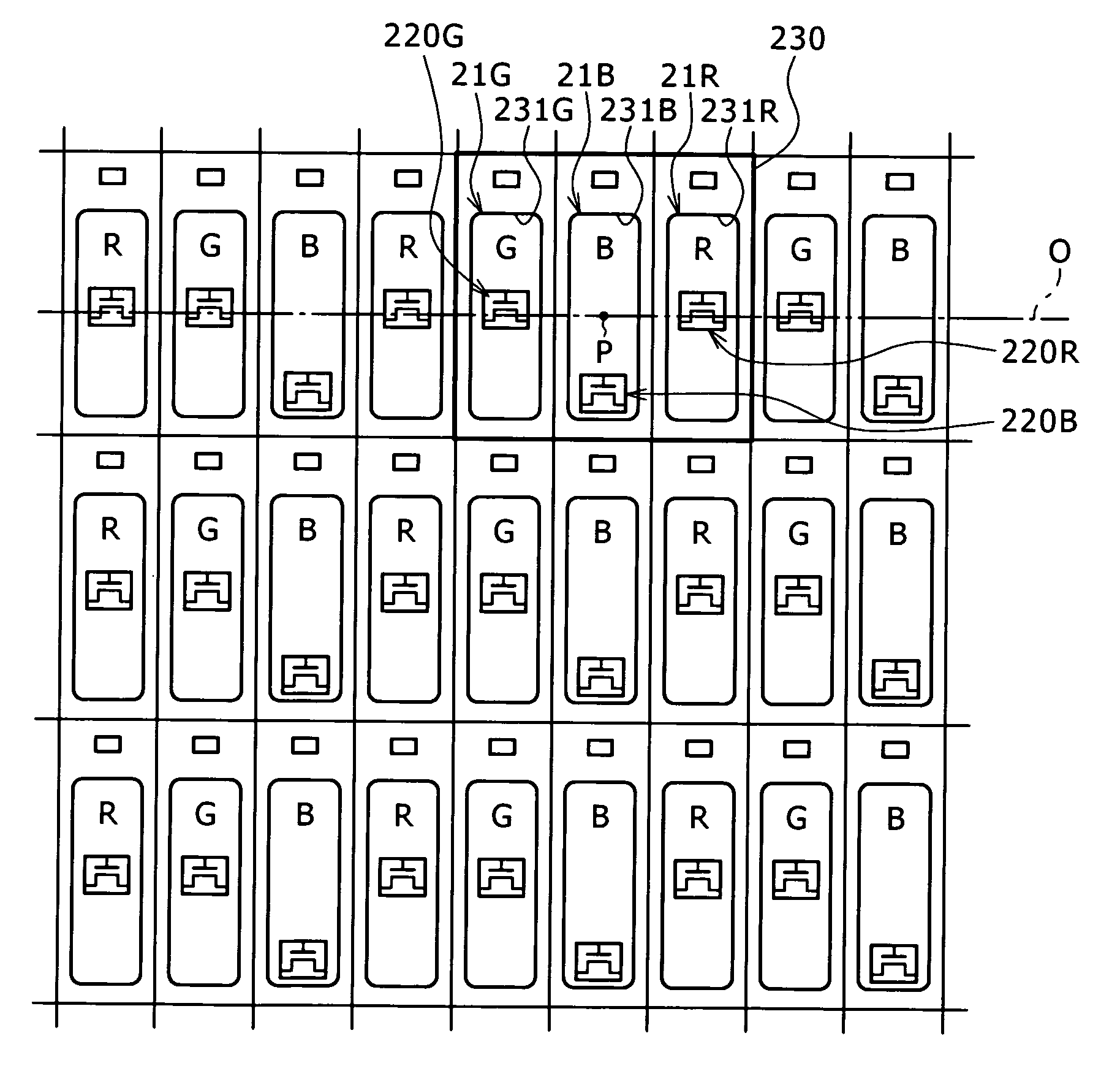
[0145]FIG. 13 is a plan view conceptually showing a layout structure according to a third embodiment. In FIG. 13, same parts as in FIG. 11 are identified by the same reference numerals.

[0146]In the present third embodiment, in a pixel arrangement of pixels (sub-pixels) 20R, 20G, and 20B of RGB repetitively arranged along a row direction (direction of arrangement of pixels of a pixel row), three pixels 20G, 20B, and 20R with the pixel 20B in the middle form a unit of one pixel. The organic EL element 21B may be a surface light source or a point light source.

[0147]Description in the following will be made of a case where a point light source is used as the organic EL element 21B. When the organic EL element 21B is a point light source, the light emission point P of the organic EL element 21B can be considered to be the center of the window 231B of the organic EL element 21B. Blue light emitted from the light emission point P of the organic EL element 21B can be considered to irradiate...


PUM


Abstract

Disclosed herein is a display device in which light emitting elements of a plurality of colors including a light emitting element emitting blue light are formed in each pixel on a substrate on which a transistor is formed for each sub-pixel, and a plurality of pixels formed with sub-pixels of the plurality of colors as a unit are arranged in a form of a matrix, wherein relative positional relation between transistors of sub-pixels of respective light emission colors including blue light and a light emitting section of a light emitting element emitting the blue light is laid out such that distances between the transistors of the sub-pixels of the respective light emission colors including the blue light and the light emitting section of the light emitting element emitting the blue light are equal to each other for the respective colors.

Description

BACKGROUND OF THE INVENTION[0001]1. Field of the Invention[0002]The present invention relates to a display device, a method of laying out light emitting elements, and an electronic device, and particularly to a flat-panel type display device in which pixels are arranged two-dimensionally in the form of a matrix, a method of laying out light emitting elements in the display device, and an electronic device having the display device.[0003]2. Description of the Related Art[0004]Recently, flat-panel type display devices in which pixels (pixel circuits) are arranged in the form of a matrix have spread rapidly in a field of display devices displaying images. As one of the flat-panel type display devices, there is a display device using a current-driven type electrooptic element whose light emission luminance changes according to the value of a current flowing through the device as light emitting elements of pixels. As a current-driven type electrooptic element, an organic EL (Electro Lumi...

Claims


Application Information

Patent Timeline
Patent Type & Authority Applications(United States)
IPC IPC(8): G09G5/10G09G3/34
CPCG09G3/3233G09G2300/0852G09G2320/0233G09G2320/043H01L27/3216H01L27/3262H01L27/326H01L27/3213H01L27/3211H10K59/351H10K59/352H10K59/353H10K59/1213H10K59/12H10K59/35H10K59/121H10K59/131H10K59/1216G09G2300/0452G09G2300/0842G09G3/3266G09G2300/0443G09G2300/0819G09G3/2074G09G2310/0289G09G2320/0626G09G3/2003G09G2320/045
Inventor MINAMI, TETSUOUCHINO, KATSUHIDE
Owner SONY CORP
Why Eureka
Try Eureka