Environmental Protection Coating System and Method

a technology of environmental protection and coating system, applied in the direction of resistive material coating, liquid/solution decomposition chemical coating, superimposed coating process, etc., can solve the problems of particulates or other contaminants, easy to attack the circuit board assembly, etc., and achieve the effect of little impact on circuit performan

Active Publication Date: 2009-11-26
RAYTHEON CO
View PDF29 Cites 42 Cited by
  • Summary
  • Abstract
  • Description
  • Claims
  • Application Information

AI Technical Summary

Benefits of technology

[0005]Embodiments of the disclosure may provide numerous technical advantages. Some, none, or all embodiments may benefit from the below described advantages. According to one embodiment, an environmental protection coating system may be provided for discrete electrical components or other assembly level features of a circuit board assembly during the assembly level phase of production. These discrete electrical components or other assembly level features may render the circuit board assembly susceptible to moisture attack, particulates or other contaminants. The environmental protection coating system of the present disclosure includes a dielectric layer made of a dielectric material that may be applied in a relatively consistent thickness to protect the discrete electrical components or other assembly level features from moisture or other harmful contaminants with relatively little impact on circuit performance.

Problems solved by technology

These discrete electrical components or other assembly level features may render the circuit board assembly susceptible to moisture attack, particulates or other contaminants.

Method used


Image

  • Environmental Protection Coating System and Method
  • Environmental Protection Coating System and Method
  • Environmental Protection Coating System and Method

Examples


embodiment 2

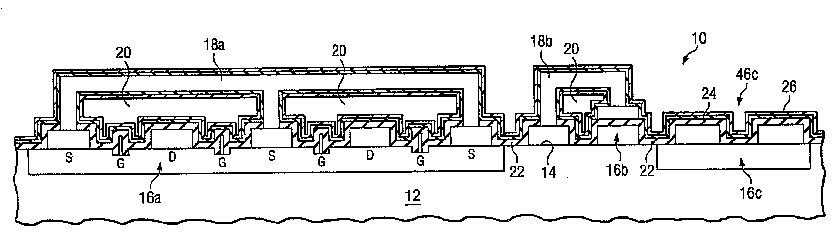
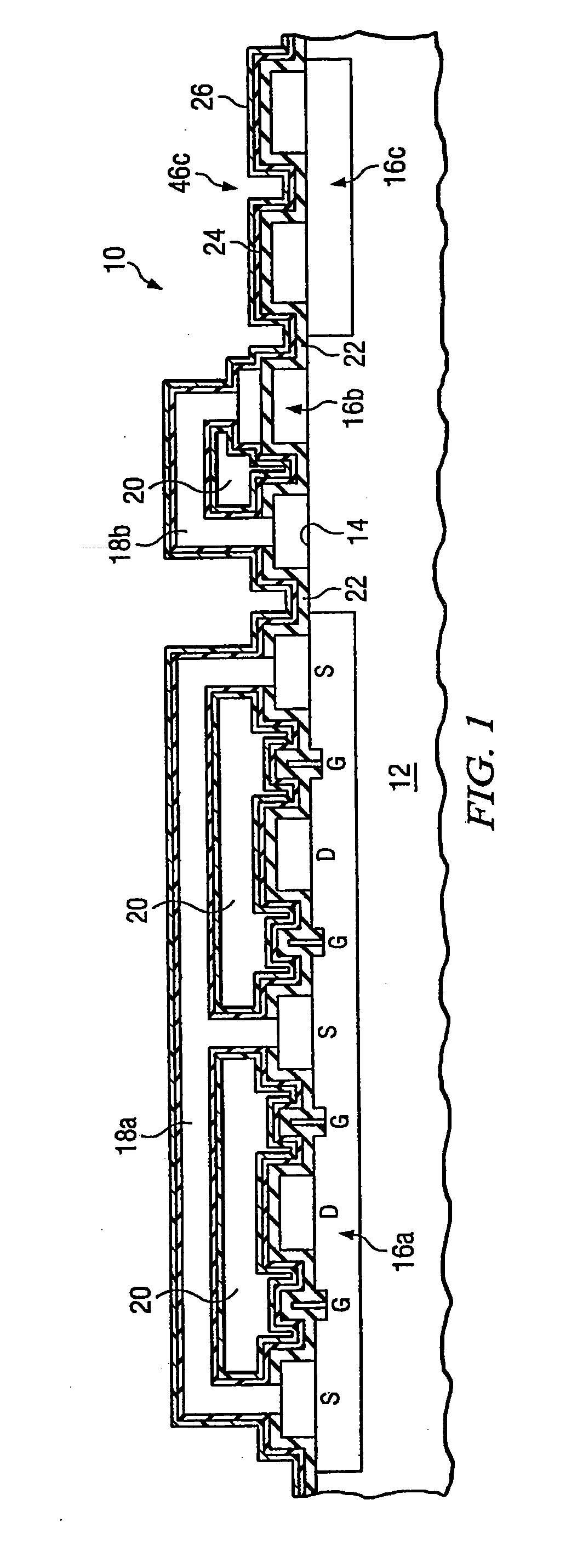
[0037 provides first 22 and second 24 protective dielectric layers formed of alumina. The second protective dielectric layer 24 covers unprotected additional components 18 such as air bridges and thick metal lines, which may be formed after the first protective dielectric layer 22 is applied. Embodiment 2 may also be desirable in hermetic or less severe humidity environments where protection against conductive or corrosive solid, liquid or gases materials may be present.

[0038]Embodiments 3 and 4 provide a third dielectric layer 26 that may be formed of silica or parylene F, parylene HT®, or other fluorinated parylene-like film as described above. The third dielectric layer 26 formed of silica or parylene F, parylene HT®, or other fluorinated parylene-like films protects the first 22 and / or second 24 protective dielectric layers from high humidity, extended humidity and / or condensed moisture which may break down the first 22 and / or second 24 protective dielectric layers 24 and expose...

embodiment 5

[0039 utilizes parylene F or parylene HT® as the second protective dielectric layer 24 of FIG. 1. Parylene F or parylene HT® covers unprotected additional features, such as air bridges and thick metal lines that may be formed after the first protective dielectric layer 22. The parylene F or parylene HT® also protects the underlying first protective dielectric layer 22 from being dissolved or attacked by moisture condensation. Parylene F or parylene HT® has the advantage of having a lower dielectric constant compared to silica or other inorganic materials and lower than most organic materials.

[0040]FIGS. 4A through 4D are cross-sectional drawings shown during various phases of manufacture of a circuit device 40 according to the teachings of the present disclosure. Circuit device 40 is generally analogous to circuit device 10 in FIG. 1. In FIG. 4A, a substrate 42 having a substrate surface 44 is shown with gate recess and gate metal applied for a number of transistor fingers 46a, cap ...

embodiment 1a

[0060 shows second protective dielectric layer 156 made of alumina. Application of the second protective dielectric layer 156 at the assembly level may provide enhanced environmental protection compared to known organic dielectrics and hence may minimize dielectric loading effects on components added at the assembly level. Such effects become increasingly important as the frequency of operation increases to microwave and millimeter wave frequencies.

[0061]Embodiment 1b utilizes a second protective dielectric layer 156 made of parylene F or parylene HT® with no third dielectric layer 158. In this particular embodiment, an adhesion promoter may be applied prior to application of the second protective dielectric layer 156. Embodiment 1b may provide relatively little electrical impact to the operation of the circuit board assembly 160 due to the low dielectric constant of parylene F or parylene HT®. Embodiment 1c utilizes a second protective dielectric layer 156 made of silica with no th...


PUM

PropertyMeasurementUnit
thicknessaaaaaaaaaa
dielectric constantaaaaaaaaaa

Abstract

A method includes providing a circuit board having an outer surface, the outer surface configured with a plurality of discrete electrical components that are each manufactured independently of one another, and coating the outer surface and the plurality of discrete electrical components with a first protective dielectric layer. The method further includes coating the first protective dielectric layer with a second dielectric layer. The second dielectric layer includes a dielectric material having a modulus of elasticity less than 3.5 Giga-Pascal (GPa), a dielectric constant less than 2.7, a dielectric loss less than 0.002, a breakdown voltage strength in excess of 2 million volts / centimeter (MV / cm), a temperature stability to 3000 Celsius, a defect densities less than 0.5 / centimeter, a pinhole free in films greater than 50 Angstroms, and is capable of being deposited conformally over and under 3D structures with thickness uniformity less than or equal to 10%.

Description

RELATED APPLICATIONS[0001]This application is a divisional of application Ser. No. 11 / 848,891, filed Aug. 31, 2007, entitled Environmental Protection Coating System and Method, which claims the benefit of priority under 35 U.S.C. § 119(e) of U.S. Provisional Application Ser. No. 60 / 888,715, entitled Environmental Protection Coating System and Method, filed Feb. 7, 2007.TECHNICAL FIELD OF THE DISCLOSURE[0002]This disclosure relates generally to environmental protection coatings, and more particularly, to an environmental protection coating system and method of manufacturing the same.BACKGROUND OF THE DISCLOSURE[0003]Circuit devices having electrical components that are integrally formed on a substrate and circuit board assemblies comprised of active and passive devices have enjoyed wide acceptance due to the wide variety of uses they may provide. Uses for these circuit devices and circuit board assemblies may include applications where operation in a protected environment is not read...

Claims


Application Information

Patent Timeline
Patent Type & Authority Applications(United States)
IPC IPC(8): B05D5/12
CPCH01L23/3192Y10T29/49146H01L24/83H01L2224/73265H01L2224/83801H01L2224/83851H01L2224/8592H01L2924/01004H01L2924/0781H01L2924/1423H01L2924/19041H05K3/284H05K2201/0179H05K2201/0195H05K2203/1322H01L2924/01019H01L23/4821Y10T29/49124Y10T29/49982Y10T29/49155H01L2924/1305H01L2924/00011H01L2224/293H01L2224/2929H01L2224/48137H01L2924/3512H01L2924/00H01L2224/29075H01L2924/00014H01L2924/14H01L2224/45014H01L21/76832H01L21/76834H01L21/7682H01L2924/206
Inventor BEDINGER, JOHN M.MOORE, MICHAEL A.
Owner RAYTHEON CO
Why Eureka
Try Eureka