Semiconductor package device, semiconductor package structure, and fabrication methods thereof

Active Publication Date: 2009-12-03
SILICONWARE PRECISION IND CO LTD
View PDF60 Cites 27 Cited by
  • Summary
  • Abstract
  • Description
  • Claims
  • Application Information

AI Technical Summary

Benefits of technology

[0017]Therefore, the present invention mainly involves providing a wafer having a plurality of silicon substrates, wherein each of the silicon substrates has a first surface and an opposed second surface and a plurality of TSVs filled with a conductive material; disposing a plurality of semiconductor chips on the first surfaces of the silicon substrates with the semiconductor chips electrically connected to the TSVs; forming an encapsulant on the first surfaces of the silicon substrates to encapsulate the semiconductor chips; forming a hard component on the encapsulant; forming a plurality of conductive elements on the second surfaces of the silicon substrates; and then performing a singulation process to the wafer so as to separate the silicon substrates from each other, thereby forming a plurality of semiconductor package devices with

Problems solved by technology

However, since the semiconductor chips 30 have different thicknesses, the wafer 20 cannot be disposed in a flat manner, which can lead to p

Method used


Image

  • Semiconductor package device, semiconductor package structure, and fabrication methods thereof
  • Semiconductor package device, semiconductor package structure, and fabrication methods thereof
  • Semiconductor package device, semiconductor package structure, and fabrication methods thereof

Examples


Example

[0021]The following illustrative embodiments are provided to illustrate the disclosure of the present invention, these and other advantages and effects can be apparent to those skilled in the art after reading the disclosure of this specification. The present invention may also be implemented and applied according to other embodiments, and the details may be modified based on different views and applications without departing from the spirit of the invention.

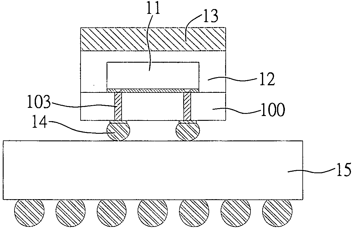
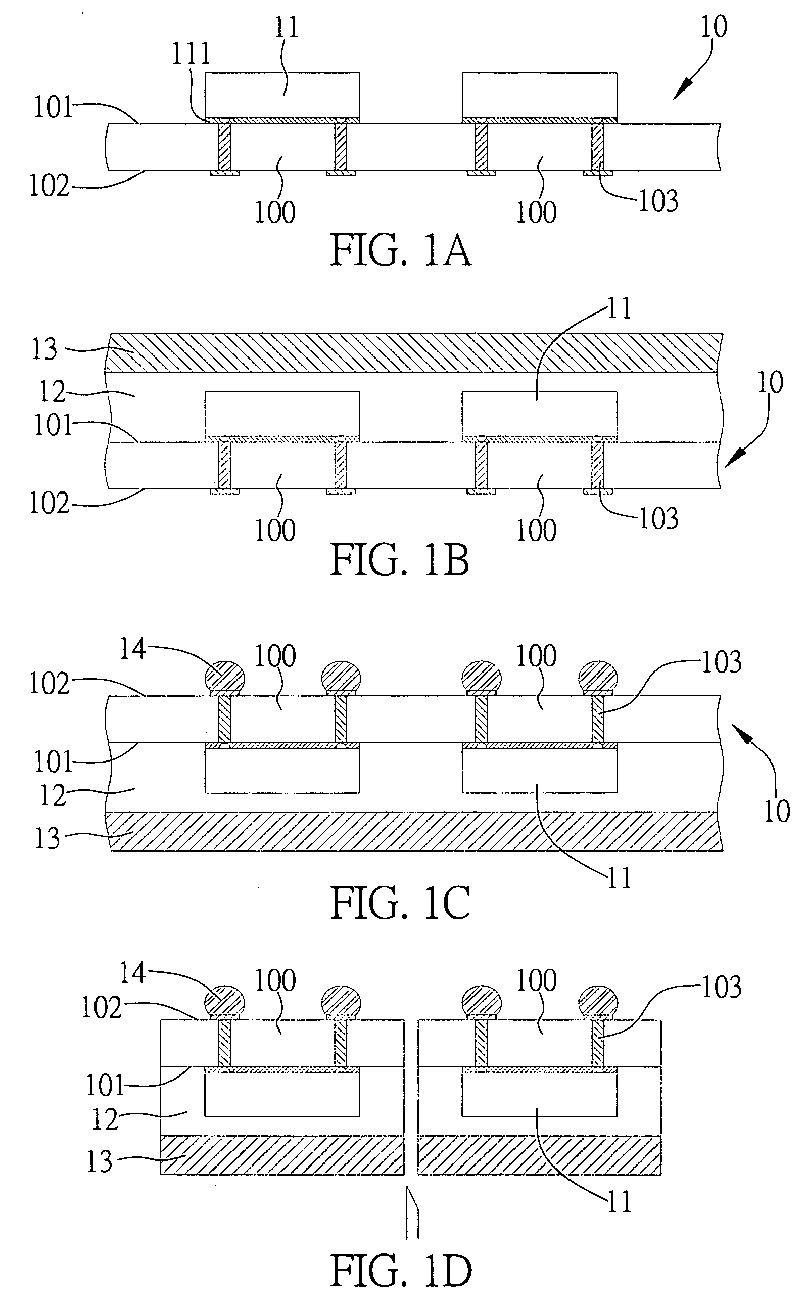
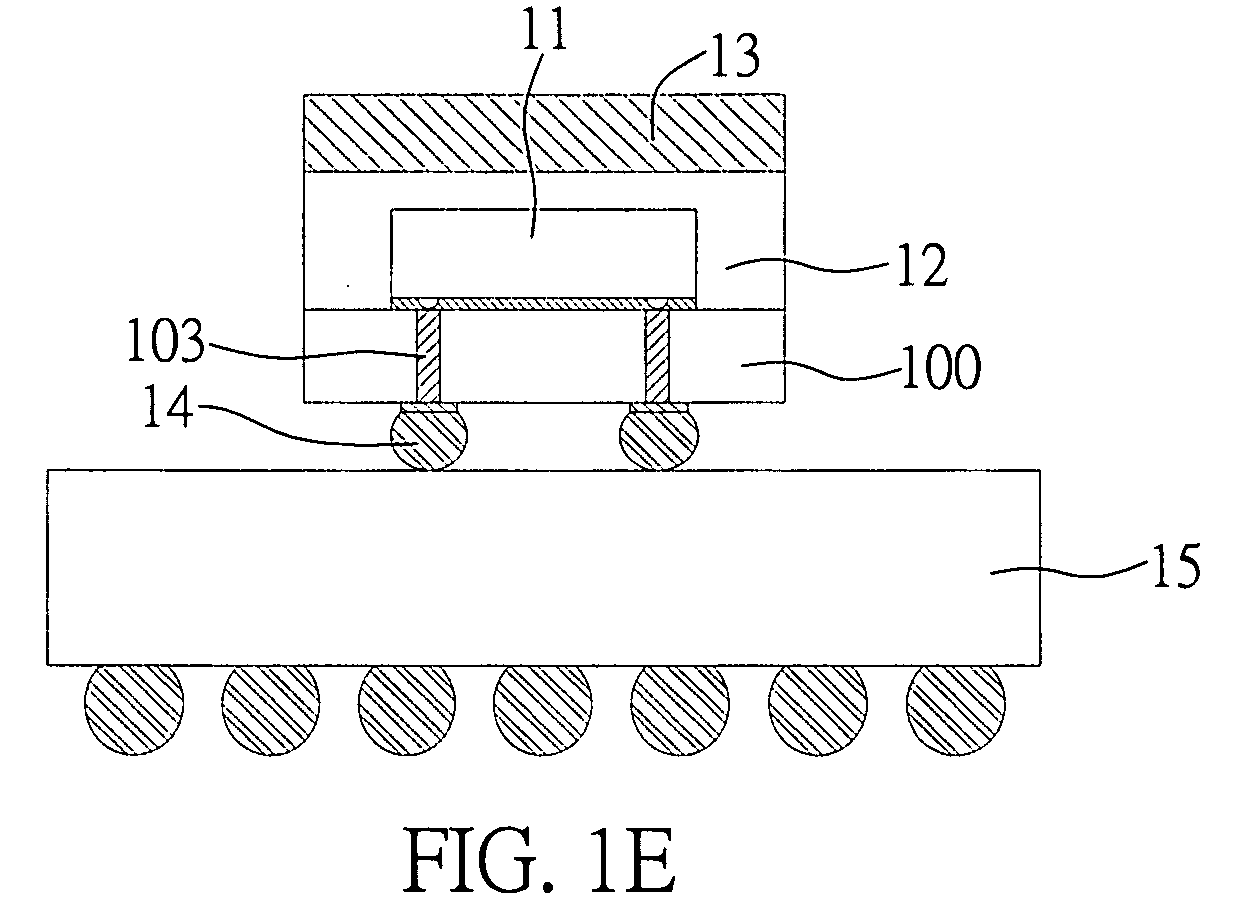
[0022]FIGS. 1A to 1D are sectional views showing a semiconductor package device and a fabrication method thereof according to the present invention.

[0023]As shown in FIG. 1A, a wafer 10 having a plurality of silicon substrates 100 is provided. Each of the silicon substrates 100 has a first surface 101 and a second surface 102 opposed to the first surface 101. A plurality of TSVs 103 is formed in each of the silicon substrates 100, wherein the TSVs 103 are filled with a conductive material. That is, at least a through hole is for...


PUM


Abstract

A semiconductor package device, a semiconductor package structure, and fabrication methods thereof are provided, which mainly includes disposing a plurality of semiconductor chips on a wafer formed with TSVs (Through Silicon Vias) and electrically connecting the semiconductor chips to the TSVs; encapsulating the semiconductor chips with an encapsulant; and disposing a hard component on the encapsulant. The hard component ensures flatness of the wafer during a solder bump process and provides support to the wafer during a singulation process such that the wafer can firmly lie on a singulation carrier, thereby overcoming the drawbacks of the prior art, namely difficulty in mounting of solder bumps, and difficulty in cutting of the wafer.

Description

BACKGROUND OF THE INVENTION[0001]1. Field of the Invention[0002]The present invention relates generally to semiconductor package devices, semiconductor package structures, and fabrication methods thereof, and more particularly to a semiconductor package device with TSVs (Through Silicon Vias), a semiconductor package structure, and fabrication methods thereof.[0003]2. Description of Related Art[0004]Along with the development of electronic products and the requirement for high integration of semiconductor chips, TSV technique based on deep silicon etching has been proposed and disclosed in such as U.S. Pat. No. 5,270,261 and No. 5,202,754.[0005]Referring to FIGS. 2A to 2E, a conventional fabrication method of a semiconductor device with TSVs is shown. As shown in the drawings, a wafer 20 with a plurality of openings 201 formed on a first surface thereof is provided, wherein the openings 201 are filled with a metal material 21, and solder pads 22 are formed on the metal material 21 a...

Claims


Application Information

Patent Timeline
IPC IPC(8): H01L23/522H01L23/532H01L23/28H01L23/31
CPCH01L21/486H01L23/3128H01L23/49827H01L24/97H01L2224/97H01L2924/01029H01L2924/01079H01L2924/01082H01L2924/15311H01L2924/01033H01L2924/01087H01L2224/16225H01L2224/32225H01L2224/73204H01L2924/157H01L2224/16235H01L2924/3511H01L23/4334H01L23/3135H01L2924/00H01L2224/81H01L23/31
Inventor CHIANG, CHENG-CHIACHANG, CHIN-HUANGHUANG, CHIEN-PINGHUANG, CHIH-MINGHUANG, JUNG-PIN
Owner SILICONWARE PRECISION IND CO LTD
Why Eureka
Try Eureka