Organic light emitting display device

a technology of light-emitting display and organic material, which is applied in the direction of discharge tube luminescnet screen, discharge tube/lamp details, final product manufacturing, etc., can solve the problems of reducing the yield of oled devices manufactured using such a process and devoted a lot of effort to achieve maximum efficiency, and achieves the effect of improving productivity

Active Publication Date: 2009-12-03
SAMSUNG DISPLAY CO LTD
View PDF5 Cites 26 Cited by
  • Summary
  • Abstract
  • Description
  • Claims
  • Application Information

AI Technical Summary

Benefits of technology

[0008]An aspect of an embodiment of the present invention is directed toward an organic light emittin

Problems solved by technology

Thus, a lot of effort has been devoted to obtaining maximal efficiency and maximal brightness of OLEDs by controlling the thicknesses of organic films.
This process is com

Method used


Image

  • Organic light emitting display device
  • Organic light emitting display device
  • Organic light emitting display device

Examples


Embodiment Construction

[0023]In the following detailed description, only certain exemplary embodiments of the present invention are shown and described, by way of illustration. As those skilled in the art would recognize, the invention may be embodied in many different forms and should not be construed as being limited to the embodiments set forth herein. Also, in the context of the present application, when an element is referred to as being “on” another element, it can be directly on the another element or be indirectly on the another element with one or more intervening elements interposed therebetween. Like reference numerals designate like elements throughout the specification.

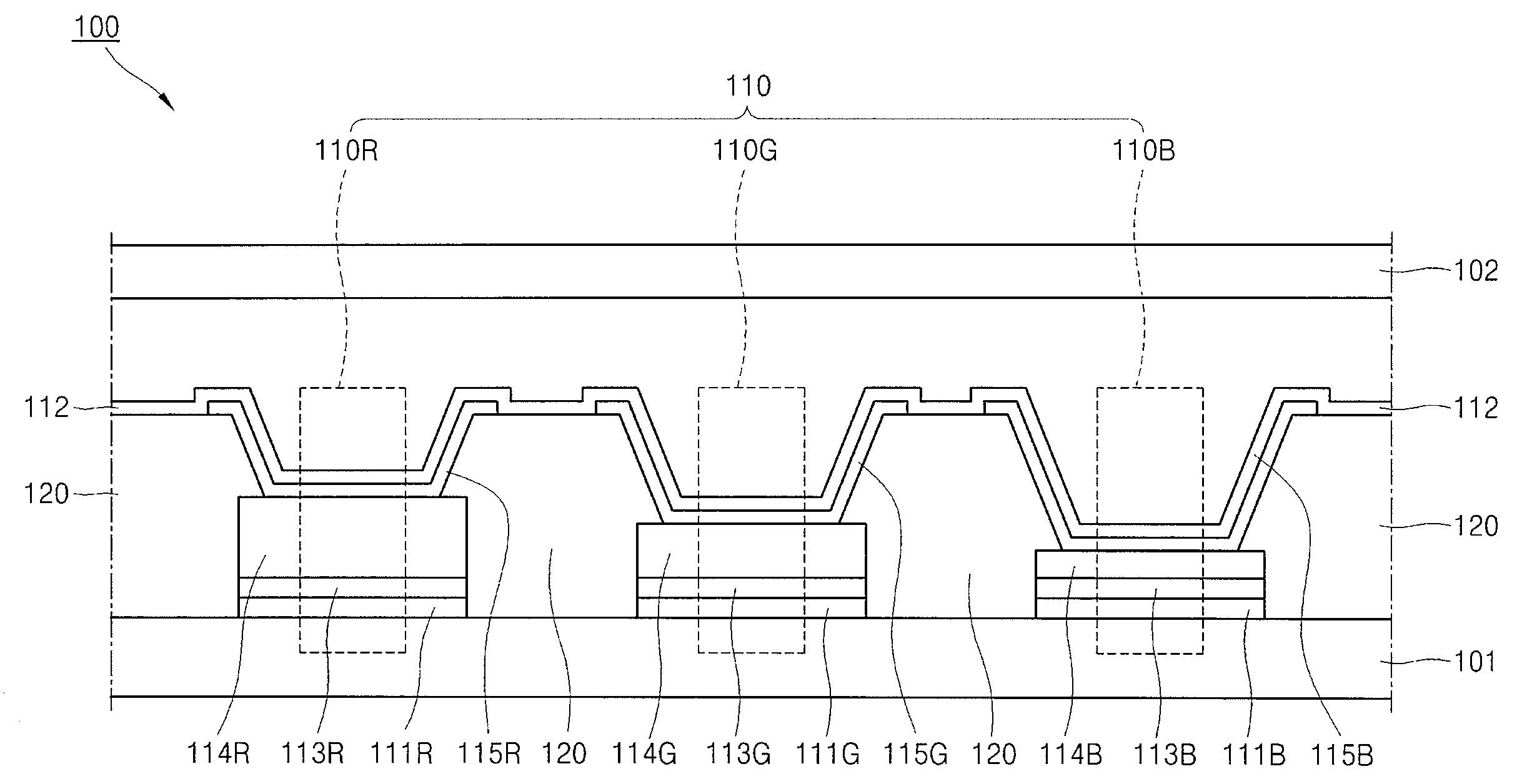
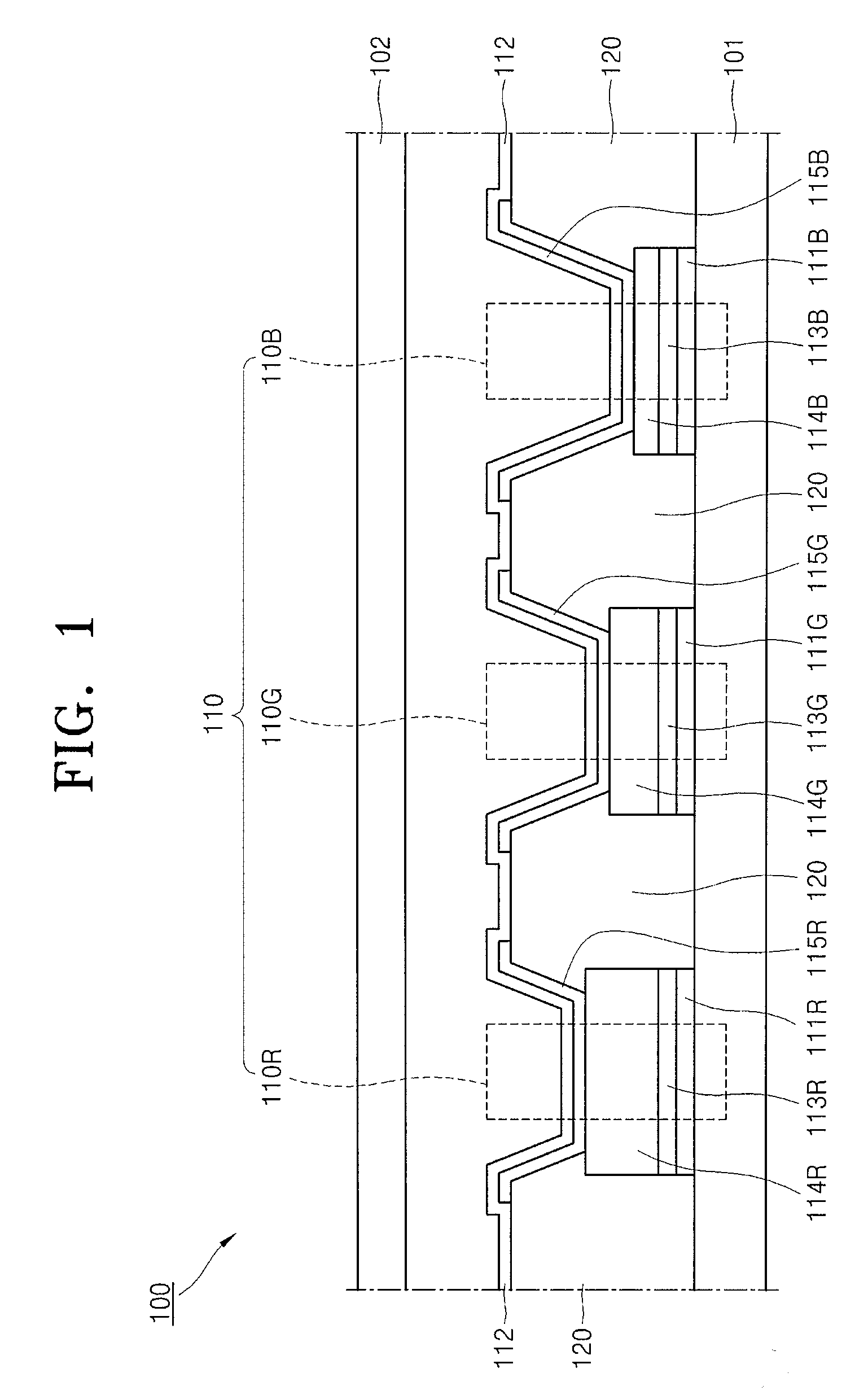
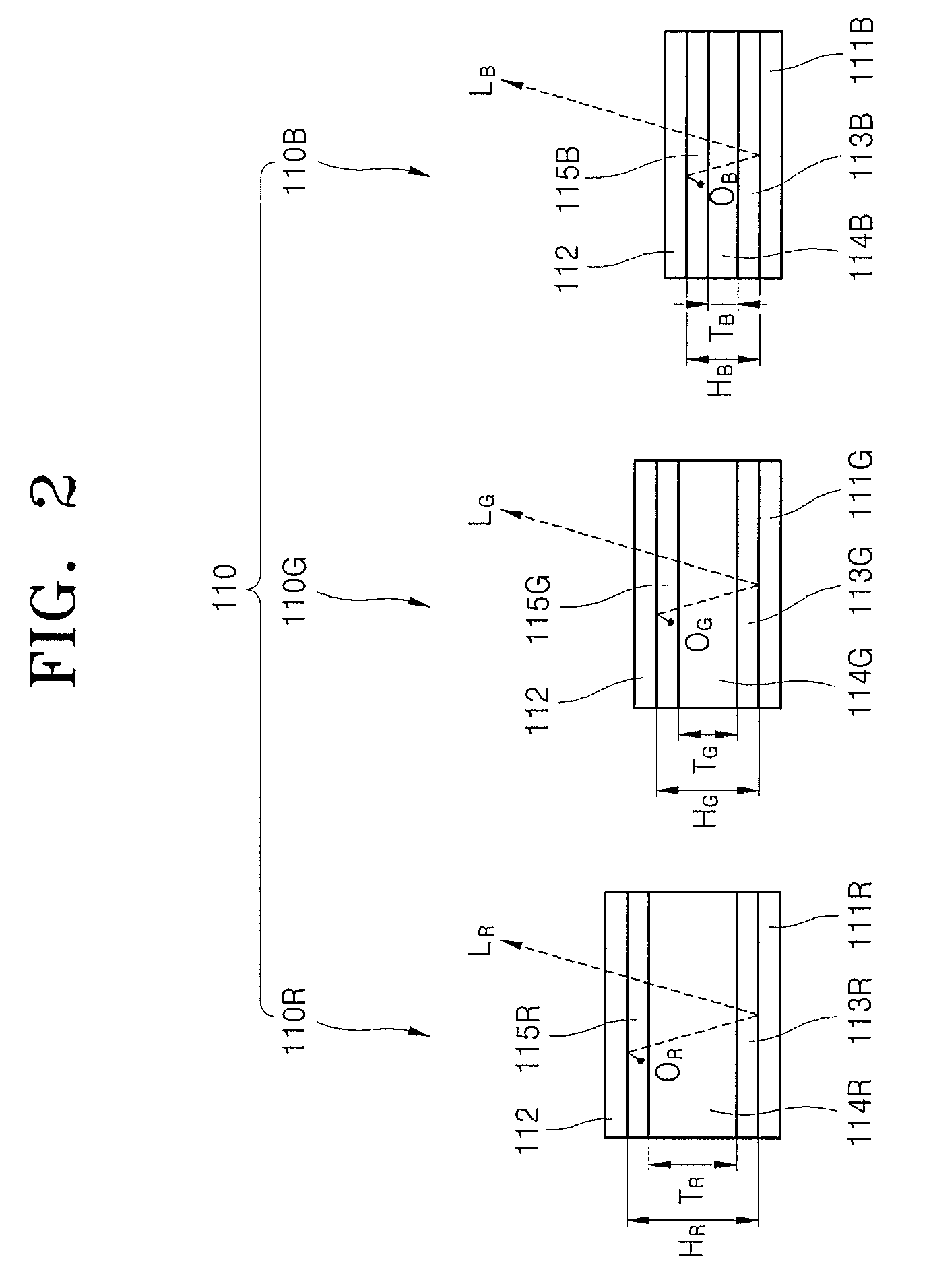
[0024]FIG. 1 is a schematic cross-sectional view of a top emission organic light emitting display (OLED) device 100 according to an embodiment of the present invention. FIG. 2 is a schematic cross-sectional view illustrating an organic light emission unit 110, including first, second, and third pixel units 110R, 110G, and 110B,...


PUM


Abstract

An organic light emitting display (OLED) device having an organic light emission unit, the organic light emitting unit including a first electrode layer on a substrate, a second electrode layer on the first electrode layer, and an organic layer between the first electrode layer and the second electrode layer, the OLED device including a first auxiliary electrode layer between the organic layer and the first electrode layer. The organic light emission unit is divided into first, second, and third pixel units. Each of the first, second, and third pixel units includes a second auxiliary electrode layer between the organic layer and the first auxiliary electrode layer. The second auxiliary electrode layers of the first, second and third pixel units are formed to have different thicknesses respectively, so that light beams emitted from the first, second and third pixel units can be provided with a resonance effect.

Description

CROSS-REFERENCE TO RELATED PATENT APPLICATION[0001]This application claims priority to and the benefit of Korean Patent Application No. 10-2008-0049673, filed on May 28, 2008, in the Korean Intellectual Property Office, the entire content of which is incorporated herein by reference.BACKGROUND OF THE INVENTION[0002]1. Field of the Invention[0003]The present invention relates to an organic light emitting display (OLED) device.[0004]2. Description of the Related Art[0005]OLED devices are self-emissive display devices including an anode, a cathode, and an organic light emission layer disposed between the cathode and the anode. When a voltage is applied to an OLED device, electrons injected from the cathode and holes injected from the anode are recombined within the organic light emission layer, thereby generating light. OLED devices can be designed to be light and thin as compared with cathode ray tubes (CRTs) or liquid crystal displays (LCDs), and are receiving attention as next-gener...

Claims


Application Information

Patent Timeline
IPC IPC(8): H01J1/62
CPCH01L51/5265H01L51/5215Y02E10/549Y02P70/50H10K50/816H10K50/852H01L27/1233H01L2924/097H01L2924/068H10K59/35H10K30/82H10K59/10
Inventor YOON, JI-HWANLEE, KWAN-HEE
Owner SAMSUNG DISPLAY CO LTD
Why Eureka
Try Eureka