Flash Memory Device and Method for Manufacturing the Same

a flash memory and memory chip technology, applied in the field of flash memory chips, can solve the problems of deterioration of the operation properties of transistors, reduced critical dimension size, and rapid reduction of cell curren

Active Publication Date: 2009-12-03
SK HYNIX INC
View PDF5 Cites 72 Cited by
  • Summary
  • Abstract
  • Description
  • Claims
  • Application Information

AI Technical Summary

Problems solved by technology

However, the decrease in critical dimension size has been limited by limitation in exposing resolution for pattern transcription.
Also, as the size of the cell gate is decreased to tens nm, for example to less than 40 nm, cell current is rapidly reduced and this causes deterioration in operation properties of the transistor.
Such limitation in exposing resolution or reduction in cell current limits decrease in memory cell size and consequently limits increase in integration degree of a memory device.

Method used


Image

  • Flash Memory Device and Method for Manufacturing the Same
  • Flash Memory Device and Method for Manufacturing the Same
  • Flash Memory Device and Method for Manufacturing the Same

Examples


Embodiment Construction

[0031]While the subject matter of this patent is susceptible to various modifications and alternative forms, certain embodiments are shown by way of example in the drawings and these embodiments will be described in detail herein. It will be understood, however, that this disclosure is not intended to limit the invention to the particular forms described, but to the contrary, the invention is intended to cover all modifications, alternatives, and equivalents falling within the spirit and scope of the invention defined by the appended claims. Throughout the following detailed description, similar reference numbers refer to respective similar elements in all figures of the drawings.

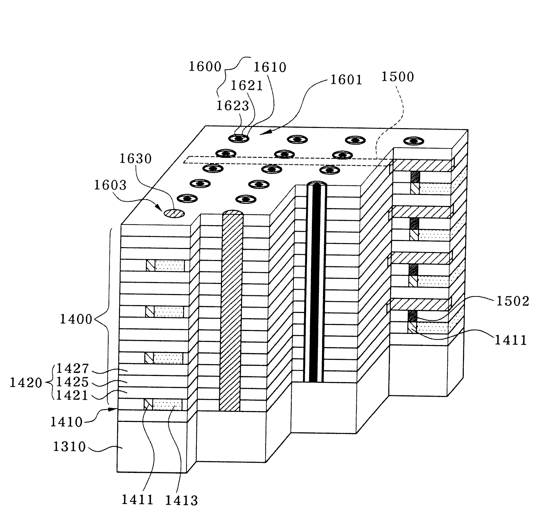
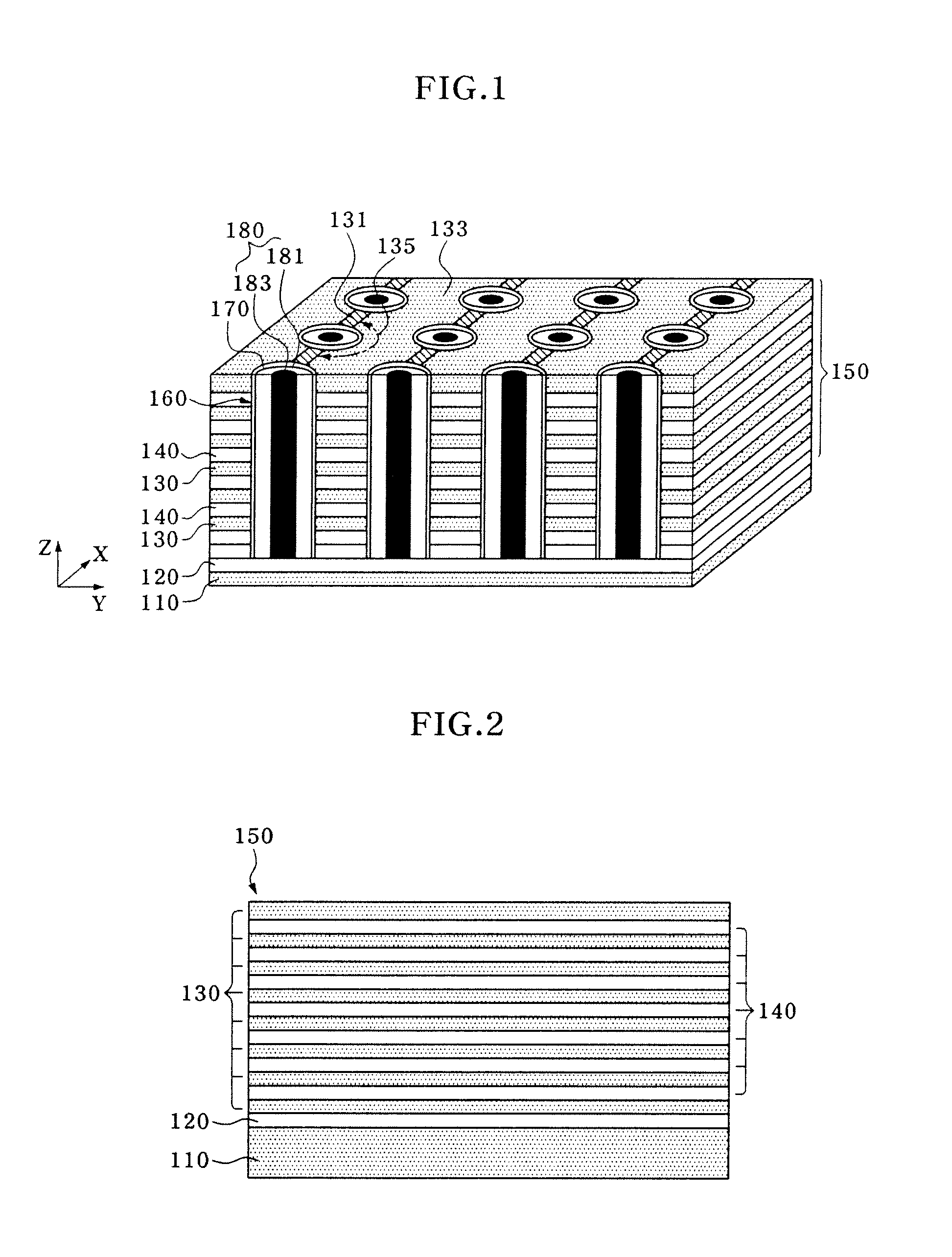
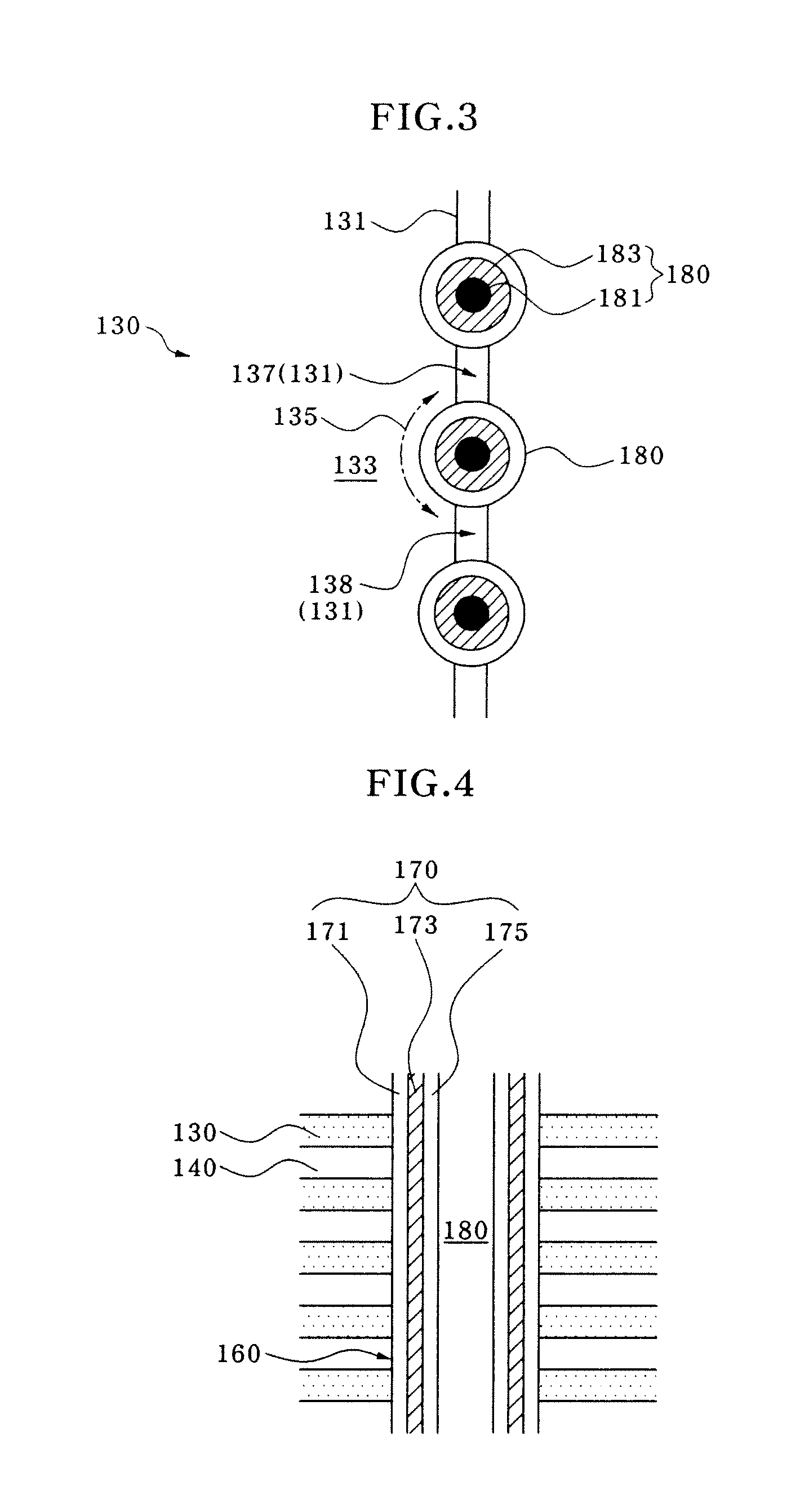
[0032]In the embodiments of the invention, a semiconductor layer including a channel area and a junction area is formed over a wafer or a substrate and then an interlayer isolation layer for insulating between devices is formed over the semiconductor layer. With repeated stacking of the semiconductor layer ...


PUM


Abstract

A flash memory device includes a substrate, a cell stack having a semiconductor layer, in which junction areas for setting areas therebetween to channel areas are formed in a shape of a stripe, and an interlayer isolation layer for insulating the semiconductor layer, wherein the semiconductor layer and the interlayer isolation layer are repeatedly stacked. The flash memory device further includes an array of gate columns penetrating through the cell stack, perpendicular to the substrate and cutting through the junction areas to dispose the junction areas at both sides thereof, and a trap layered stack introduced into an interface between the gate column and the cell stack to store charge.

Description

CROSS-REFERENCE TO RELATED APPLICATIONS[0001]This patent claims priority to Korean patent application numbers 10-2008-0049571, 10-2008-0049572 and 10-2008-0049581, filed on May 28, 2008 respectively which are incorporated by reference in theirs entirety.TECHNICAL FIELD[0002]This patent relates to a semiconductor device, and more particularly, to a flash memory device and a method for manufacturing the same.BACKGROUND OF THE INVENTION[0003]Demand for a non-volatile memory device that maintains the stored state of information even when power is interrupted has been increased. As an example of the non-volatile memory device, a flash memory device in which memory cells are connected as a NAND string by sharing junctions is widely used to store massive information. As increase in memory capacity of the NAND flash memory device is required, decrease in size of a cell transistor that forms the memory cell has been largely required and increase in integration degree by this decrease in size...

Claims


Application Information

Patent Timeline
Patent Type & Authority Applications(United States)
IPC IPC(8): G11C11/34H01L21/00
CPCG11C5/02G11C16/0483H01L27/11582H01L27/11565H01L27/11578H01L27/0688H10B43/10H10B43/20H10B43/27
Inventor SHIN, HACK SEOBPARK, KYOUNG HWANHONG, YOUNG OKPARK, YU JIN
Owner SK HYNIX INC
Why Eureka
Try Eureka