Wafer level camera module and method of manufacturing the same

a technology of camera module and camera body, which is applied in the direction of semiconductor/solid-state device manufacturing, electrical apparatus, semiconductor devices, etc., can solve the problems of difficult to obtain high-quality images and almost impossible to apply them to an effective mass production process, so as to facilitate mass production and reduce material and process costs

Inactive Publication Date: 2009-12-17
SAMSUNG ELECTRO MECHANICS CO LTD
View PDF2 Cites 37 Cited by
  • Summary
  • Abstract
  • Description
  • Claims
  • Application Information

AI Technical Summary

Benefits of technology

[0013]The present invention has been invented in order to overcome the above-described problems, it is, therefore, an object of the present invention to provide a wafer level camera module and a method of manufacturing the same capable of securing an exact position error in a wafer level, facilitating mass production and reducing material and process costs by bonding substrates through anodic bonding.

Problems solved by technology

However, conventionally, an adhesive was used to assemble a wafer level package of the image sensor and a lens group, which increases an error due to a thickness of an adhesion layer and thus it is difficult to obtain a high quality image and it is almost impossible to apply it to an effective mass production process.

Method used


Image

  • Wafer level camera module and method of manufacturing the same
  • Wafer level camera module and method of manufacturing the same
  • Wafer level camera module and method of manufacturing the same

Examples


Embodiment Construction

[0025]Hereinafter, a matter regarding to an operation effect including a technical configuration to achieve the object of a wafer level camera module and a method of manufacturing the same in accordance with the present invention will be clearly appreciated through the following detailed description with reference to the accompanying drawings illustrating preferable embodiments of the present invention.

[0026]A Structure of a Wafer Level Camera Module

[0027]Hereinafter, a wafer level cameral module in accordance with an embodiment of the present invention will be described in detail with reference to FIG. 1.

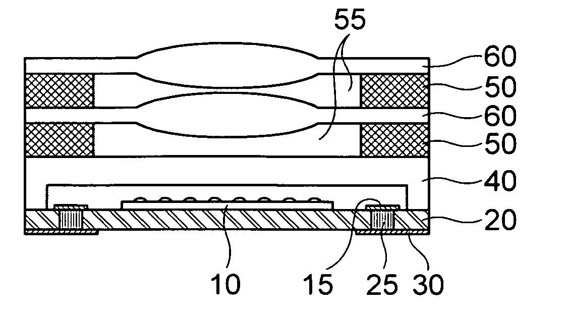
[0028]FIG. 1 is a cross-sectional view showing a structure of a wafer level camera module in accordance with the embodiment of the present invention.

[0029]As shown in FIG. 1, in accordance with the embodiment of the present invention, a wafer level cameral module includes a wafer level package 45(referring to “45” in FIG. 2) in which a transparent member 40 is bonded to a wafer 20 ...


PUM


Abstract

The present invention relates to a wafer level camera module and a method of manufacturing the same and provides a wafer level camera module including a wafer provided with an image sensor on a top surface; a transparent member bonded to the wafer through anodic bonding to seal the image sensor; a spacer bonded to the transparent member through the anodic bonding by including a window to expose the image sensor; and a wafer lens bonded to the spacer through the anodic bonding to cover the window of the spacer and further a method of manufacturing the same.

Description

CROSS-REFERENCE TO RELATED APPLICATIONS[0001]This application claims the benefit of Korean Patent Application No. 10-2008-0056789 filed with the Korea Intellectual Property Office on Jun. 17, 2008, the disclosure of which is incorporated herein by reference.BACKGROUND OF THE INVENTION[0002]1. Field of the Invention[0003]The present invention relates to a wafer level camera module and a method of manufacturing the same; and, more particularly, to a wafer level camera module and a method of manufacturing the same to bond substrates through anodic bonding.[0004]2. Description of the Related Art[0005]Currently, a portable terminal such as a mobile phone and a PDA(Personal Digital Assistant) is used as multi-convergence for a music, a movie, a TV and a game as well as a simple call function with development of a technique thereof and the most representative one of things to lead development of the multi-convergence is a camera module. Such a camera module has been changed from existing 3...

Claims


Application Information

Patent Timeline
Patent Type & Authority Applications(United States)
IPC IPC(8): H01L31/18H01L31/0232
CPCH01L27/14618H01L27/14685H01L27/14625H01L2924/0002H01L2924/00H04N23/00
Inventor JEUNG, WON KYULEE, SEUNG SEOUP
Owner SAMSUNG ELECTRO MECHANICS CO LTD
Why Eureka
Try Eureka