
Wiring board and wiring board manufacturing method

Inactive Publication Date: 2009-12-24
PANASONIC CORP
View PDF8 Cites 8 Cited by
  • Summary
  • Abstract
  • Description
  • Claims
  • Application Information

AI Technical Summary

Benefits of technology

[0010]The present invention has been made in consideration of the conventional wiring board problems, and an object of the invention is to provide a wiring board and a wiring board manufacturing method that are capable of suppressing the spreading of liquid droplets discharged by an ink-jet method.
[0078]a treatment step of treating the porous membrane member with a predetermined solution after forming the first wiring pattern, to thereby reduce a thickness of the porous membrane member.
[0082]According to the present invention, there can be provided a wiring board and a wiring board manufacturing method that are capable of suppressing the spreading of liquid droplets discharged by an ink-jet method.

Problems solved by technology

However, when an ink-jet method is used, it is necessary to set the viscosity of the electrically conductive nanoparticle paste that is discharged to a low viscosity in order to prevent the nozzle from blocking up, and hence there is the problem that the electrically conductive nanoparticle paste that is discharged onto a substrate spreads out, and thus the lines of a wiring pattern can only be formed at a width that is significantly greater than the diameter of the liquid droplets.
Further, because the electrically conductive nanoparticle paste that is discharged spreads after landing in a spot shape on the surface of a substrate, wiring lines can only be formed with a thickness of several microns.
Wiring lines that are formed in that manner cannot absorb a stress produced by a thermal shock or vibrations by plastic deformation, and hence a sufficient conductive adhesive strength can no longer be obtained.
Further, when wiring lines are thin, the problem arises that the resistance value thereof increases and a loss when transmitting signals or the like increases.

Method used


Image

  • Wiring board and wiring board manufacturing method
  • Wiring board and wiring board manufacturing method
  • Wiring board and wiring board manufacturing method

Examples


embodiment 1

[0134]A wiring board according to Embodiment 1 of the present invention is described hereunder. According to Embodiment 1, the structure of a wiring board on which an ink-jet wiring pattern is formed on a surface of a substrate or on a surface of another layer, on which a wiring pattern is not formed by a method (for example, a transfer method) other than an ink-jet method is described.

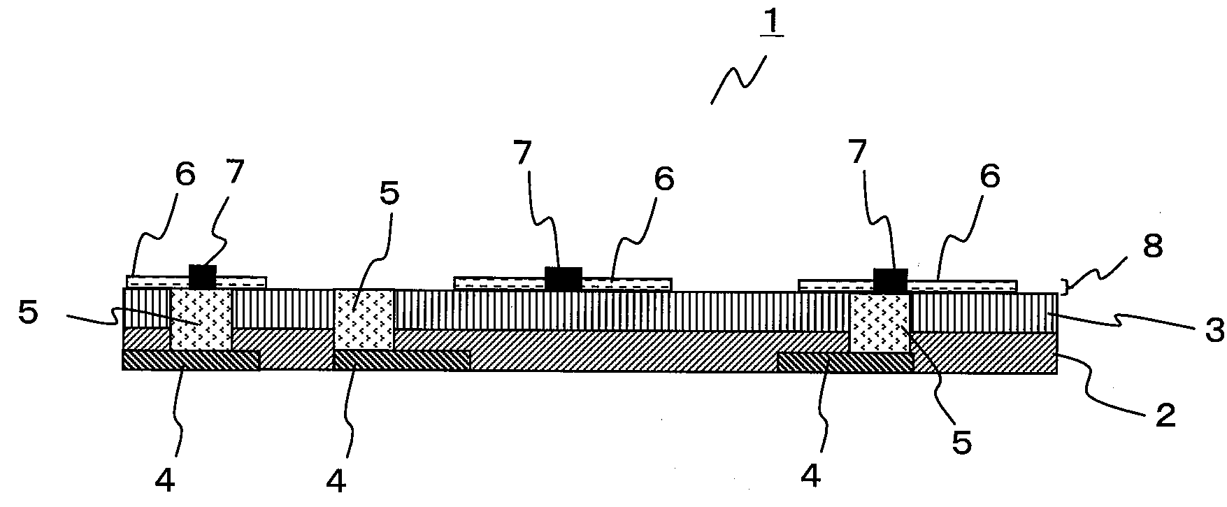
[0135]FIG. 1 is sectional configuration diagram of a wiring board 1 according to the present embodiment. As shown in FIG. 1, the wiring board 1 according to the present embodiment includes a film substrate 3 that is formed from an organic film, and a tabular substrate 2 that includes a thermosetting resin that is provided on one side of the film substrate 3.

[0136]A transferred wiring pattern 4 is formed on a surface on the opposite side to the film substrate 3 of the substrate 2. The surface of the transferred wiring pattern 4 is exposed, and the transferred wiring pattern 4 is embedded in the substra...

embodiment 2

[0192]Next, a wiring board according to Embodiment 2 of the present invention will be described.

[0193]According to the present embodiment, a wiring board is described that has a configuration in which an ink-jet wiring pattern is formed on the surface of a substrate in which a transferred wiring pattern has been formed. Although the basic structure of the wiring board of the present embodiment 2 is the-same as that of Embodiment 1, the present embodiment differs from Embodiment 1 in the respect that the porous membrane treated member 6 is arranged on the surface of a substrate in which a transferred wiring pattern has been formed. Consequently, the following description centers on the present point of difference. In this connection, in the present embodiment 2 the same symbols are used to denote constituent elements that are substantially the same as in Embodiment 1.

[0194]FIG. 12 is a sectional configuration diagram of a wiring board 20 according to the present embodiment 2. The wir...

embodiment 3

[0212]Hereunder, the configuration of a wiring board according to Embodiment 3 of the present invention is described.

[0213]According to the present embodiment a wiring board is described in which, unlike Embodiment 2, an ink-jet wiring pattern is formed on a surface of a substrate on which a wiring pattern has been formed by a method (excluding an ink-jet method) other than a transfer method.

[0214]FIG. 18(A) is a sectional configuration diagram of a wiring board 30 according to the present embodiment 3. The wiring board 30 of the present embodiment 3 includes a multilayer board 302 that is provided on a surface of the substrate 2, and a multilayer board 301 that is provided on a surface of the film substrate 3. FIG. 18(B) is a partially enlarged view of FIG. 18(A). In this connection, in the present embodiment 3 the same symbols are used to denote constituent elements that are the same as in Embodiment 2.

[0215]As shown in FIG. 18(B), the multilayer board 301 is formed of four substr...


PUM

PropertyMeasurementUnit
Fractionaaaaaaaaaa
Temperatureaaaaaaaaaa
Thicknessaaaaaaaaaa

Abstract

A wiring board is provided that suppresses spreading of liquid droplets when liquid droplets are discharged using an ink-jet method. The wiring board has a plurality of layers and includes an ink-jet wiring pattern that is formed in a soluble porous membrane member of any single layer and that includes electrically conductive nanoparticles as a principal material, and a transferred wiring pattern that does not include electrically conductive nanoparticles as a principal material. One layer among the plurality of layers is an electrically insulative substrate. Another layer among the plurality of layers is a porous membrane treated member layer including a porous membrane member at one part of a region of the other layer. The ink-jet wiring pattern is formed in the porous membrane treated member layer. The transferred wiring pattern is formed in the substrate.

Description

BACKGROUND OF THE INVENTION[0001]1. Field of the Invention[0002]The present invention relates to a wiring board and a wiring board manufacturing method.[0003]2. Related Art of the Invention[0004]Accompanying the miniaturization, thinning, and advanced functions of electronic devices in recent years, there is an increasingly stronger demand for high-density mounting of electronic components that are to be mounted on printed wiring boards, higher functionality of wiring boards on which electronic components are mounted, and miniaturization of wiring boards on which electronic components are mounted. In these circumstances, the wiring that is formed on the wiring boards is becoming more minute.[0005]However, for example in the case of using screen printing or the like, it has been difficult to create minute wiring.[0006]To solve this problem, a method has been disclosed that forms wiring patterns by selecting an ink-jet method for wiring pattern regions in which a wiring line interval ...

Claims


Application Information

Patent Timeline
IPC IPC(8): H05K1/09B05D5/12B32B38/14B05D3/10
CPCH05K1/0265Y10S977/773H05K1/0272H05K1/0393H05K3/1208H05K3/125H05K3/205H05K3/386H05K3/4069H05K3/4602H05K3/4664H05K3/4697H05K2201/0116H05K2201/0195H05K2201/0352H05K2201/0391H05K2201/068H05K2201/09036H05K2201/09136H05K2201/096H05K2201/09727H05K2203/013H05K2203/0769H05K1/0271
Inventor HIROSE, TAKAYUKITSUKAHARA, NORIHITOGOKAN, MANABU
Owner PANASONIC CORP
Features
  • Generate Ideas
  • Intellectual Property
  • Life Sciences
  • Materials
  • Tech Scout
  • Unparalleled Data Quality
  • Higher Quality Content
  • 60% Fewer Hallucinations
Learn More