Substrate processing method and substrate processing apparatus

a substrate processing and substrate technology, applied in the direction of coatings, solid-state devices, chemical vapor deposition coatings, etc., can solve the problems of low film forming rate, non-uniform film thickness, and limitations of conventional substrate processing methods and apparatuses, so as to prevent deterioration of film thickness uniformity and maintain film forming rate

Active Publication Date: 2009-12-31
KOKUSA ELECTRIC CO LTD
View PDF5 Cites 21 Cited by
  • Summary
  • Abstract
  • Description
  • Claims
  • Application Information

AI Technical Summary

Benefits of technology

[0013]An object of the present invention is to provide a substrate processing method and apparatus adapted to prevent deterioration of film thickness uniformity while maintaining the film forming rate. Specifically, an object of the present invention is to provide a substrate processing method and apparatus adapted to prevent generation of fine crystalline grains at a place such as the interface between amorphous-silicon (a-Si) and an insulating film for ensuring film thickness uniformity while maintaining the film forming rate.

Problems solved by technology

However, such conventional substrate processing methods and apparatuses have limitations, such as a low film forming rate when a silicon film is formed at a low temperature and non-uniformity in film thickness when a silicon film is formed using highly reactive gas.
That is, in the related art, if a substrate is processed by, for example, a lateral solid phase epitaxial growth method, fine crystalline grains are easily formed between amorphous silicon (a-Si) and an insulating film, and in this case, when heat treatment is performed for monocrystallization of Si, the fine crystalline grains grow and make the monocrystallization of Si difficult.
However, in the case of such a low-temperature process, the film forming rate is low.
However, in the case where highly reactive gas is used as process gas, the thickness uniformity of a film is deteriorated.
As explained above, according to the conventional substrate processing methods and apparatuses, a substrate cannot be processed with good in-plane film thickness uniformity while maintaining the film forming rate at a desired level.

Method used


Image

  • Substrate processing method and substrate processing apparatus
  • Substrate processing method and substrate processing apparatus
  • Substrate processing method and substrate processing apparatus

Examples


Embodiment Construction

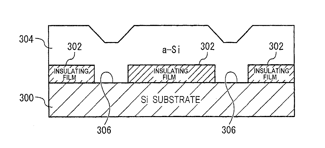
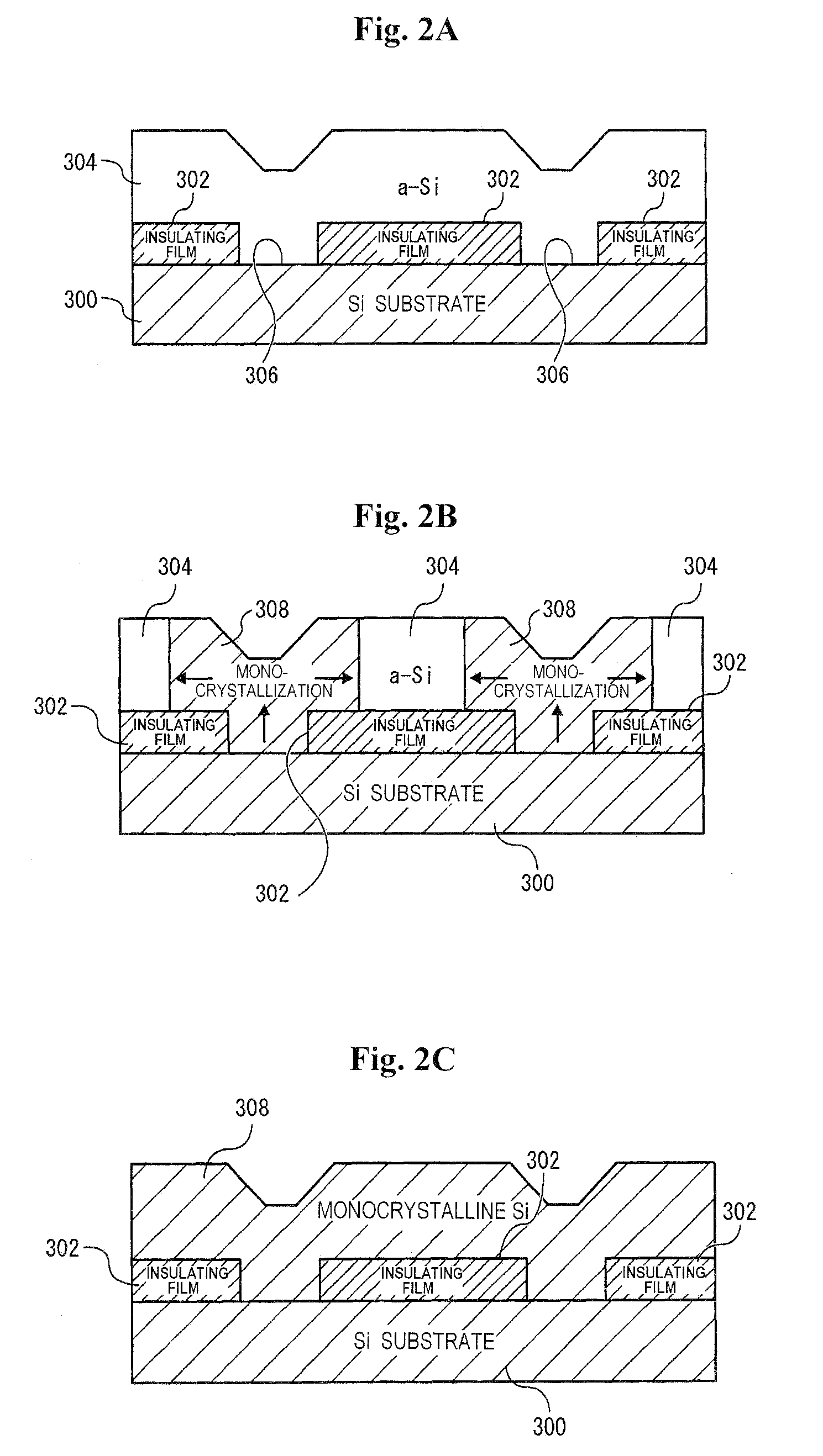
[0019]A substrate processing method and apparatus relevant to embodiments of the pressure will be described hereinafter with reference to the attached drawings.

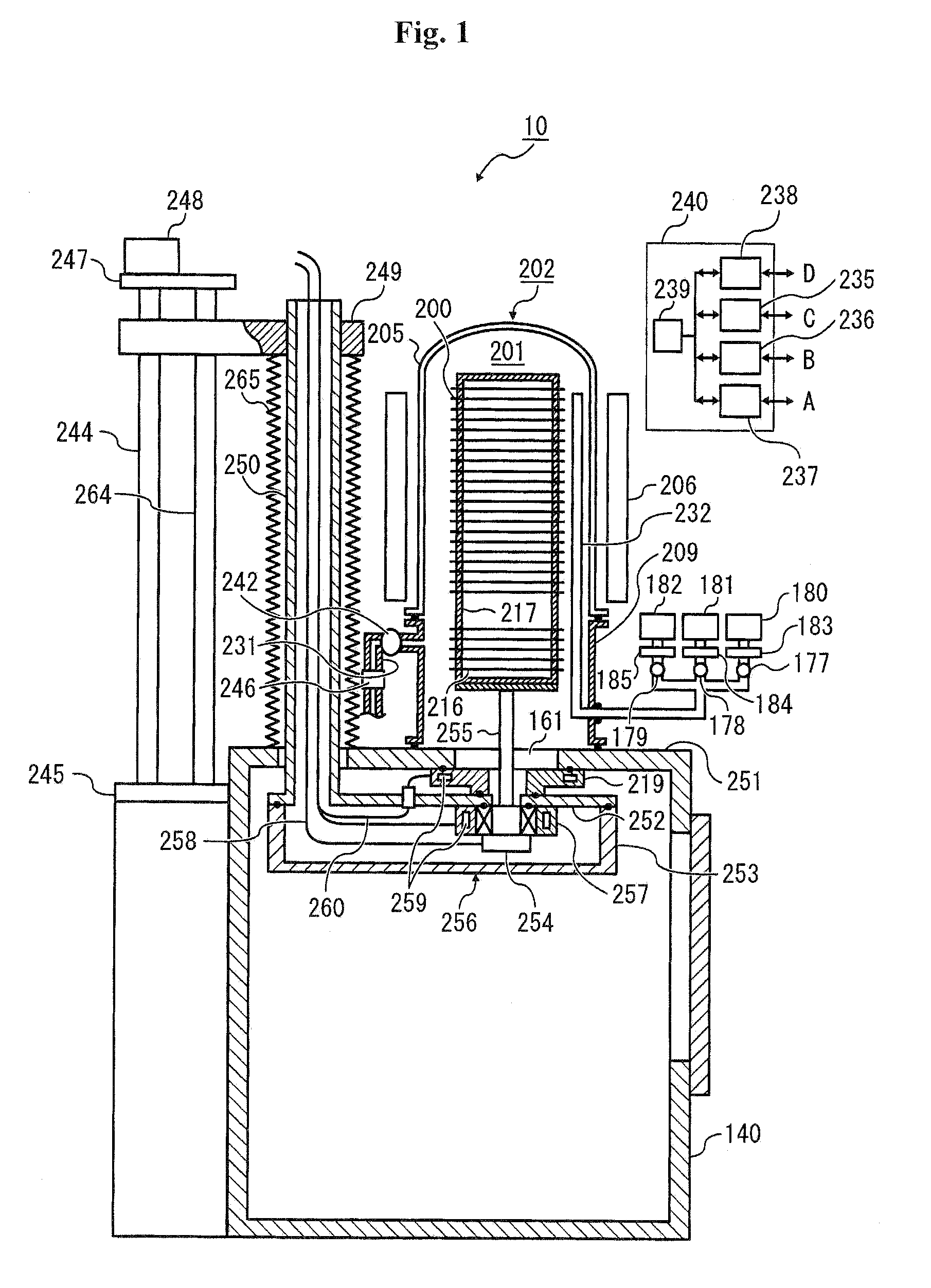
[0020]FIG. 1 illustrates a substrate processing apparatus 10 relevant to an embodiment of the present invention.

[0021]The substrate processing apparatus 10 is configured as a vertical chemical vapor deposition (CVD) apparatus for performing a substrate processing process relevant to an embodiment of the present invention.

[0022]Although the substrate processing apparatus 10 is a vertical CVD apparatus, the present invention can be applied to other substrate processing apparatuses such as a horizontal CVD apparatus and a single wafer type CVD apparatus. In addition, although the substrate processing apparatus 10 is a so-called hot-wall type apparatus, the present invention can be applied to a so-called cold-wall type apparatus.

[0023]As shown in FIG. 1, the substrate processing apparatus 10 includes a process furnace 202 and a h...


PUM


Abstract

There are provided a substrate processing method and apparatus adapted to prevent deterioration of film thickness uniformity while maintaining the film forming rate. The substrate processing method comprises: (a) accommodating a plurality of substrates in a process chamber by carrying and stacking the substrates in the process chamber, (b) forming first amorphous silicon films to a predetermined thickness by heating at least the substrates and supplying first gas, and (c) forming second amorphous silicon films to a predetermined thickness by heating at least the substrates and supplying second gas different from the first gas. The first gas is higher order gas than the second gas.

Description

CROSS-REFERENCE TO RELATED PATENT APPLICATION[0001]This U.S. non-provisional patent application claims priority under 35 U.S.C. §119 of Japanese Patent Application No. 2008-169819, filed on Jun. 30, 2008, in the Japanese Patent Office, the entire contents of which are hereby incorporated by reference.BACKGROUND OF THE INVENTION[0002]1. Field of the Invention[0003]The present invention relates to a substrate processing method and apparatus for forming an amorphous silicon film on a monocrystalline substrate having an insulating film formed on at least a surface portion thereof and an exposed silicon surface.[0004]2. Description of the Prior Art[0005]There are conventional substrate processing methods and apparatuses for forming an amorphous silicon film on a monocrystalline substrate having an insulating film formed on at least a surface portion thereof and an exposed silicon surface.[0006]However, such conventional substrate processing methods and apparatuses have limitations, such ...

Claims


Application Information

Patent Timeline
Patent Type & Authority Applications(United States)
IPC IPC(8): H01L21/365C23C16/42
CPCC23C16/24H01L21/02381H01L21/02532H01L21/02592H01L27/0688H01L21/02636H01L21/02667H01L21/8221H01L21/0262H01L21/20
Inventor MORIYA, ATSUSHIINOKUCHI, YASUHIROKUNII, YASUO
Owner KOKUSA ELECTRIC CO LTD
Why Eureka
Try Eureka