Semiconductor device

Inactive Publication Date: 2010-01-07
ABLIC INC
View PDF7 Cites 10 Cited by
  • Summary
  • Abstract
  • Description
  • Claims
  • Application Information

AI Technical Summary

Benefits of technology

[0006]It is an object of the present invention to provide a semiconductor device which is capable of relaxing stress on a semiconductor chip caused during a packaging process, and has small characteristic changes before and after the packaging process.
[0012]A difference between the characteristics of the semiconductor device formed on a wafer and the characteristics of the semiconductor device assembled in a package is caused by the following reason. A resin used for sealing the semiconductor chip in the packaging process undergoes thermal expansion or thermal contraction during subsequent heat treatment, whereby tensile stress or compressive stress is applied to the semiconductor chip, adding additional resistance such as piezoresistance to elements. According to the present invention, the buffer region is formed around elements for which accuracy is particularly required for the circuit, whereby the buffer region absorbs the stress from the package, permitting suppression of the characteristic changes of the semiconductor device before and after the packaging process.

Problems solved by technology

In such a method as described above, however, the effect for stress relaxation is obtained only in a wafer form, and it has been a problem that the stress relaxation cannot be expected in a chip form after the dicing process.

Method used


Image

  • Semiconductor device
  • Semiconductor device
  • Semiconductor device

Examples


first embodiment

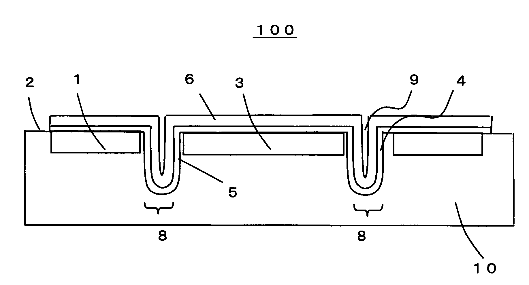
[0021]FIG. 1 is a plan view illustrating a semiconductor device 100 according to a first embodiment of the present invention. In FIG. 1, the semiconductor device 100 includes: a semiconductor element formation region 1 to which stress induces little effect in terms of characteristics; a scribe region 2; an element region 3 for which accuracy is particularly required and which is preferably prevented from receiving the stress during a packaging process; and a buffer region 8 for relaxing the stress. For example, a current mirror circuit is a circuit in which currents flowing through two current paths act to be equal to each other by utilizes the fact that the same amount of current flows in each of the paired P-channel MOS transistors. Such paired transistors as described above are required to have characteristics little different from each other, and therefore are desirably formed within the above-mentioned element region 3 which is preferably prevented from receiving the stress.

[00...

second embodiment

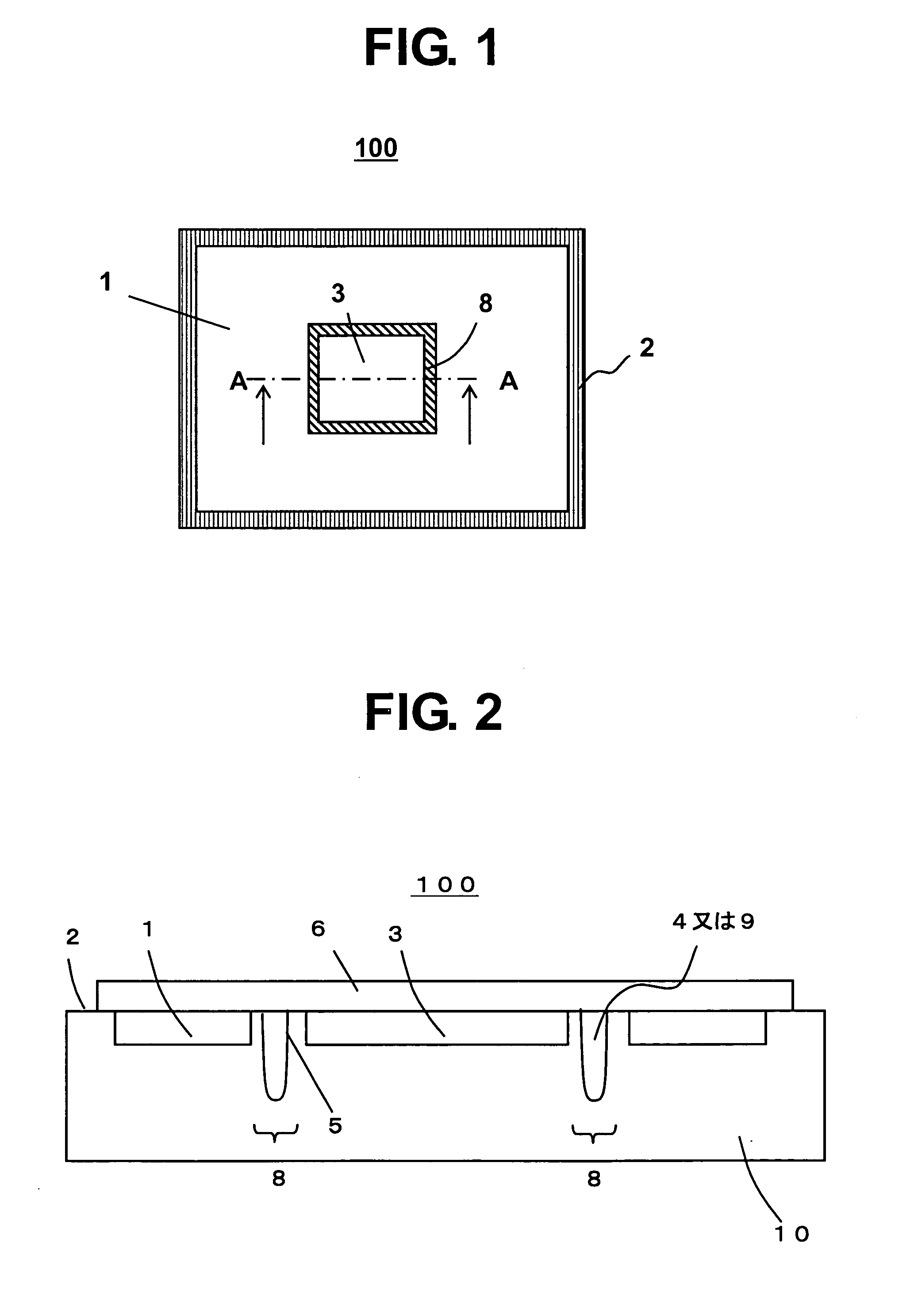
[0026]FIG. 3 is a plan view illustrating a semiconductor device 100 according to a second embodiment of the present invention. The semiconductor device 100 includes: a semiconductor element formation region 1 for elements which cause no problem even under stress; a scribe region 2; an element region 3 for elements for which accuracy is particularly required and which is preferably prevented from receiving the stress during a packaging process; a buffer region 8 for relaxing the stress; and a support region 7.

[0027]In the second embodiment, similarly to the first embodiment, the element region 3 which is preferably prevented from receiving the stress is also arranged at a center of the semiconductor device 100, and is also isolated from the surrounding semiconductor element formation region 1 by the buffer region 8. However, the support region 7 is provided for connecting the element region 3 which is preferably prevented from receiving the stress and the semiconductor element format...

third embodiment

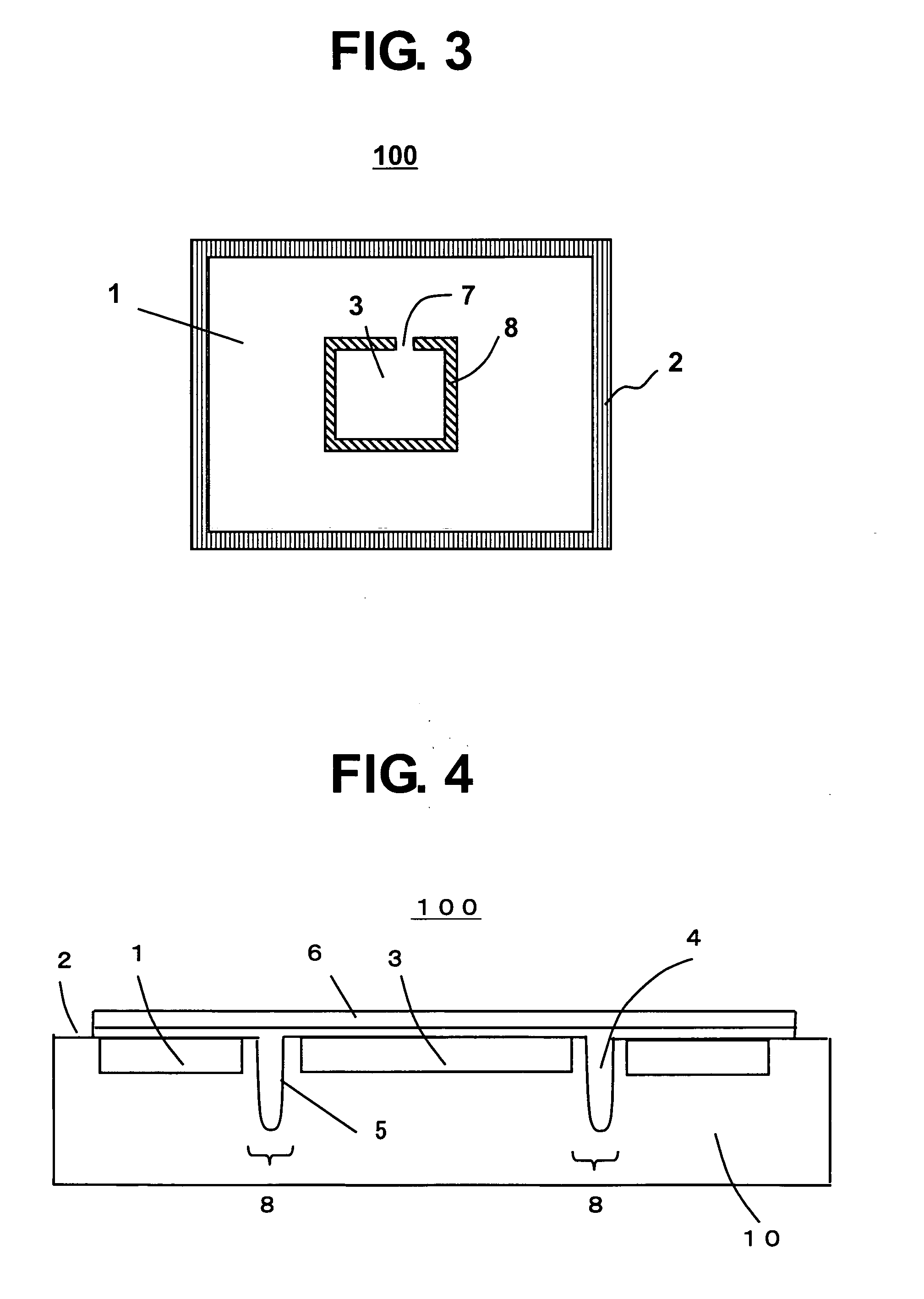
[0028]FIG. 4 is a cross-sectional view illustrating a semiconductor device 100 according to a third embodiment of the present invention. FIG. 4 is different from FIG. 2. in that the filler 4 is left on the surface of the semiconductor substrate 10. In this case, the semiconductor device 100 includes the support region 7, and an interconnection (not shown) is provided on the support region 7. As is apparent from this embodiment, the filler 4 may be embedded into the trench 5 at the formation of the protective film 6.


PUM


Abstract

A semiconductor device (100) is provided in which an element region (3) for elements for which accuracy is particularly required and which should be prevented from receiving stress from a package among elements constituting the semiconductor device (100) is surrounded by a buffer region (8) for relaxing the stress, suppressing an influence of tensile or compressive stress generated during a packaging process to thereby reduce characteristic changes before and after the packaging process.

Description

BACKGROUND OF THE INVENTION[0001]1. Field of the Invention[0002]The present invention relates to a semiconductor device capable of suppressing characteristic changes caused during a packaging process of the semiconductor device.[0003]2. Description of the Related Art[0004]Semiconductor devices formed on a wafer are cut and divided into chips through a dicing process to be assembled into packages. During a packaging process through sealing by resin and heat treatment, stress is applied to the semiconductor chip from the package, causing a warp in the semiconductor device whose characteristics are measured after the package assembling of the semiconductor device. Due to the warp, the measured characteristics of the semiconductor device may deviate from electrical characteristics of the semiconductor device measured on the wafer. As to a method for relaxing the stress, there has been proposed so far a method including forming a trench in a scribe region to thereby relax the stress in a...

Claims


Application Information

Patent Timeline
IPC IPC(8): H01L23/58
CPCH01L23/585H01L2924/0002H01L2924/00H01L23/16
Inventor KATO, SHINJIROOSANAI, JUN
Owner ABLIC INC
Why Eureka
Try Eureka