Electron emission device, electron emission type backlight unit including the same and method of fabricating the electron emission device

a backlight unit and electron emission technology, applied in the manufacture of electrode systems, electric discharge tubes/lamps, instruments, etc., can solve the problems of low post-processing efficiency, difficult to obtain desired electron emission characteristics, and low current flow, so as to improve or optimize post-processing effects, improve the uniformity between pixels

Inactive Publication Date: 2010-01-14
SAMSUNG SDI CO LTD
View PDF5 Cites 14 Cited by
  • Summary
  • Abstract
  • Description
  • Claims
  • Application Information

AI Technical Summary

Benefits of technology

[0009]Aspects of embodiments of the present invention are directed toward an electron emission device with improved uniformity between pixels and improved or optimum post-processing effects, an electron emission type backlight unit including the same, and a method of fabricating the electron emission device.

Problems solved by technology

However, when a resistance layer is formed on each electron emission source, current flow is limited and post-processing efficiency is reduced.
Thus, it is difficult to obtain desired electron emission characteristics.
In addition, since the resistance layer is deposited on each electron emission source, the process of manufacturing such an electron emission device is complicated and manufacturing costs increase.
In addition, it is difficult to change resistance values after a resistance layer has been deposited on each electron emission source.

Method used


Image

  • Electron emission device, electron emission type backlight unit including the same and method of fabricating the electron emission device
  • Electron emission device, electron emission type backlight unit including the same and method of fabricating the electron emission device
  • Electron emission device, electron emission type backlight unit including the same and method of fabricating the electron emission device

Examples


Embodiment Construction

[0029]The present invention will now be described more fully with reference to the accompanying drawings, in which exemplary embodiments of the invention are shown. Throughout this specification and the claims that follow, when an element is referred to as being “on” another element, it can be directly on the other element or be indirectly on the other element with one or more intervening elements interposed therebetween.

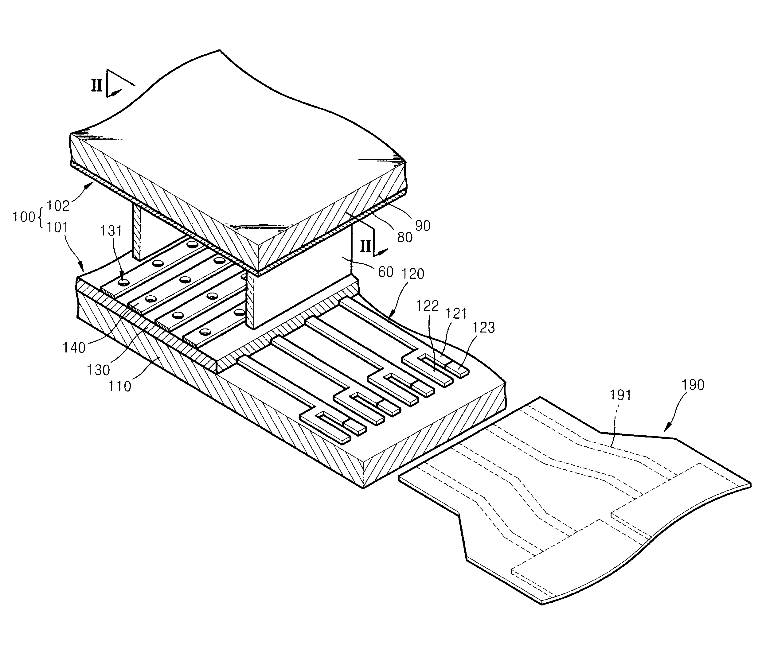
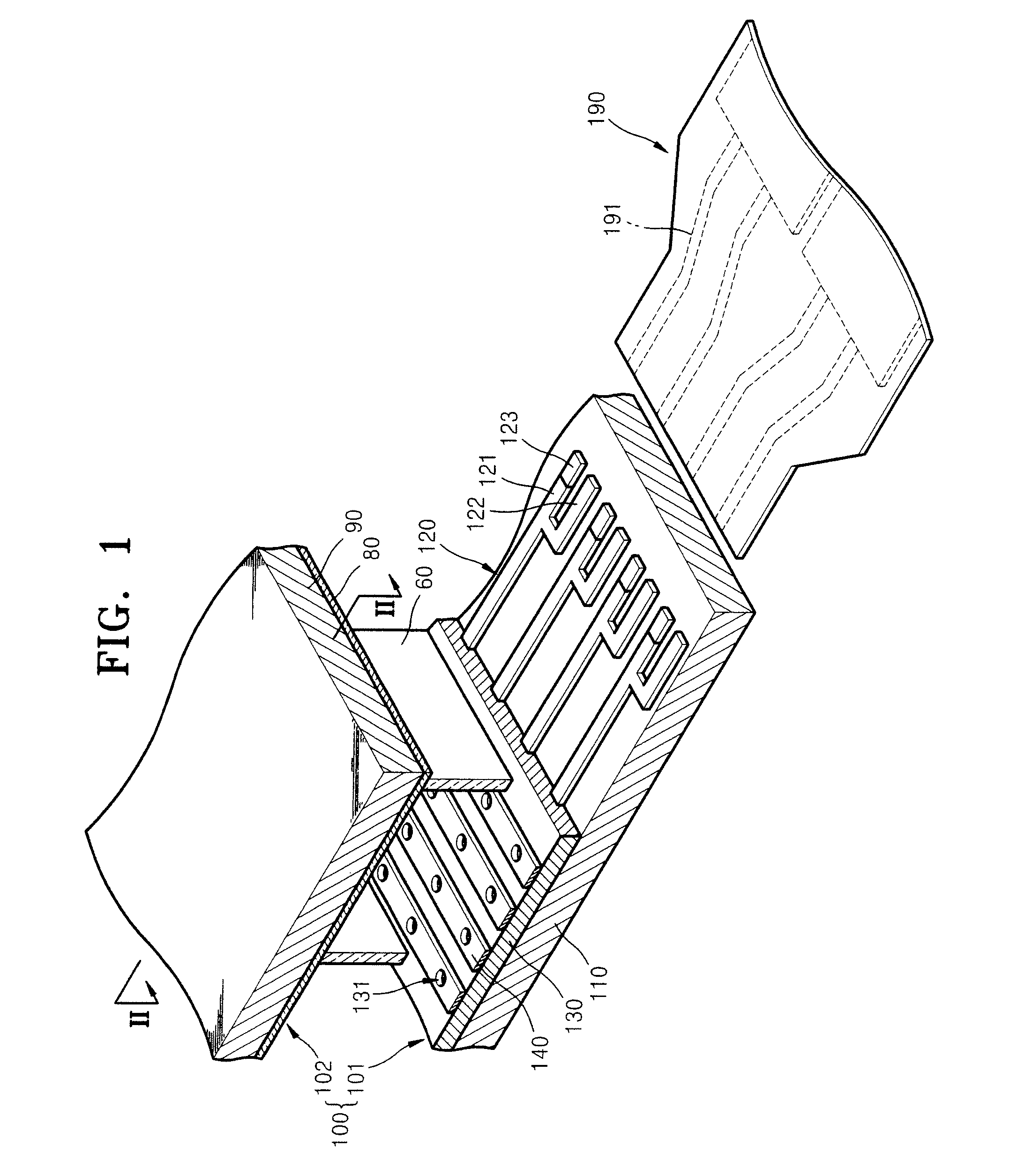
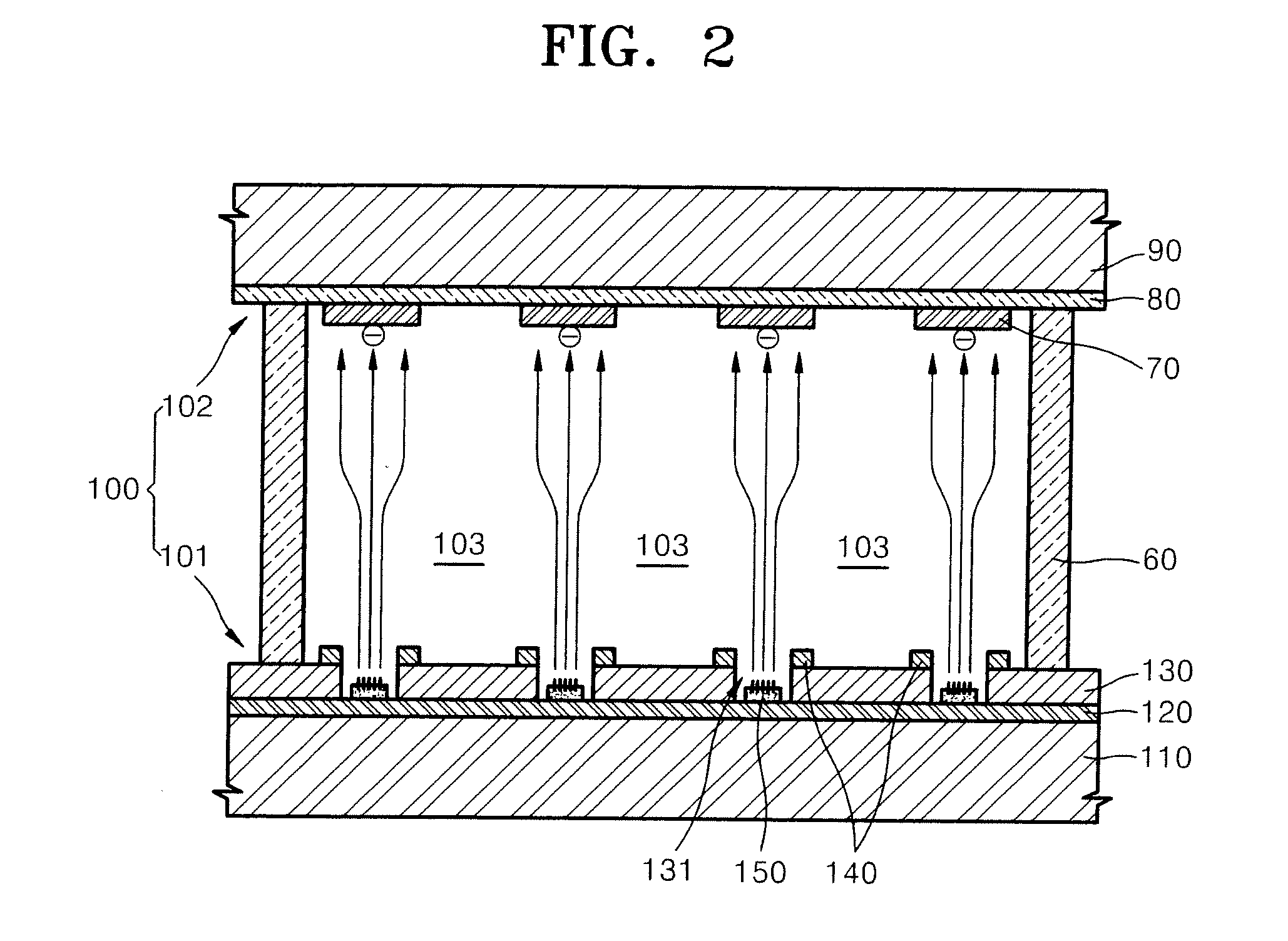
[0030]FIG. 1 is a schematic, partially-cut perspective view of a structure of an electron emission type backlight unit 100 according to an embodiment of the present invention, and FIG. 2 is a cross-sectional view of the electron emission type backlight unit 100 taken along the line II-II of FIG. 1.

[0031]Referring to FIGS. 1 and 2, the electron emission type backlight unit 100 according to the current embodiment of the present invention includes an electron emission device 101 and a front panel 102 located in front of the electron emission device 101.

[0032]The electr...


PUM


Abstract

An electron emission device, useful as a backlight unit, improves uniformity between pixels and maximizes post-processing effects. The electron emission device includes a base substrate with first electrodes extending on the base substrate, each of which includes a resistance layer formed at an end. The electron emission device also includes second electrodes electrically insulated from the first electrodes and electron emission sources formed on the first electrodes. The electron emission device is configured for current to flow through the resistance layer during a driving operation and for current to not flow through the resistance layer during an aging operation.

Description

CROSS-REFERENCE TO RELATED APPLICATION[0001]This application claims priority to and the benefit of Korean Patent Application No. 10-2008-0069302, filed on Jul. 16, 2008, in the Korean Intellectual Property Office, the disclosure of which is incorporated herein in its entirety by reference.BACKGROUND OF THE INVENTION[0002]1. Field of the Invention[0003]The present invention relates to electron emission devices.[0004]2. Description of the Related Art[0005]Electron emission devices use thermionic cathodes or cold cathodes as electron emission sources. Types of electron emission devices that use cold electrodes include field emission devices (FEDs), surface conduction emitter (SCE) devices, metal-insulator-metal (MIM) devices, metal-insulator-semiconductor (MIS) devices, and ballistic electron surface emitting (BSE) devices.[0006]FEDs operate on the principle that electrons are readily emitted due to an electric field difference in a vacuum when a material having a low work function or ...

Claims


Application Information

Patent Timeline
Patent Type & Authority Applications(United States)
IPC IPC(8): G09F13/08H01J1/00H01J9/02
CPCH01J1/02H01J9/022H01J63/06H01J29/92H01J9/445
Inventor KIM, JOO-YOUNGLEE, BYONG GON
Owner SAMSUNG SDI CO LTD
Why Eureka
Try Eureka