
Pixel and organic light emitting display device using the same

Active Publication Date: 2010-01-21
SAMSUNG DISPLAY CO LTD
View PDF4 Cites 63 Cited by
  • Summary
  • Abstract
  • Description
  • Claims
  • Application Information

AI Technical Summary

Benefits of technology

[0013]Accordingly, it is an aspect of the present invention to provide a pixel capable of improving response characteristics and displaying an image having a uniform image quality, and an organic light emitting display device using the same.
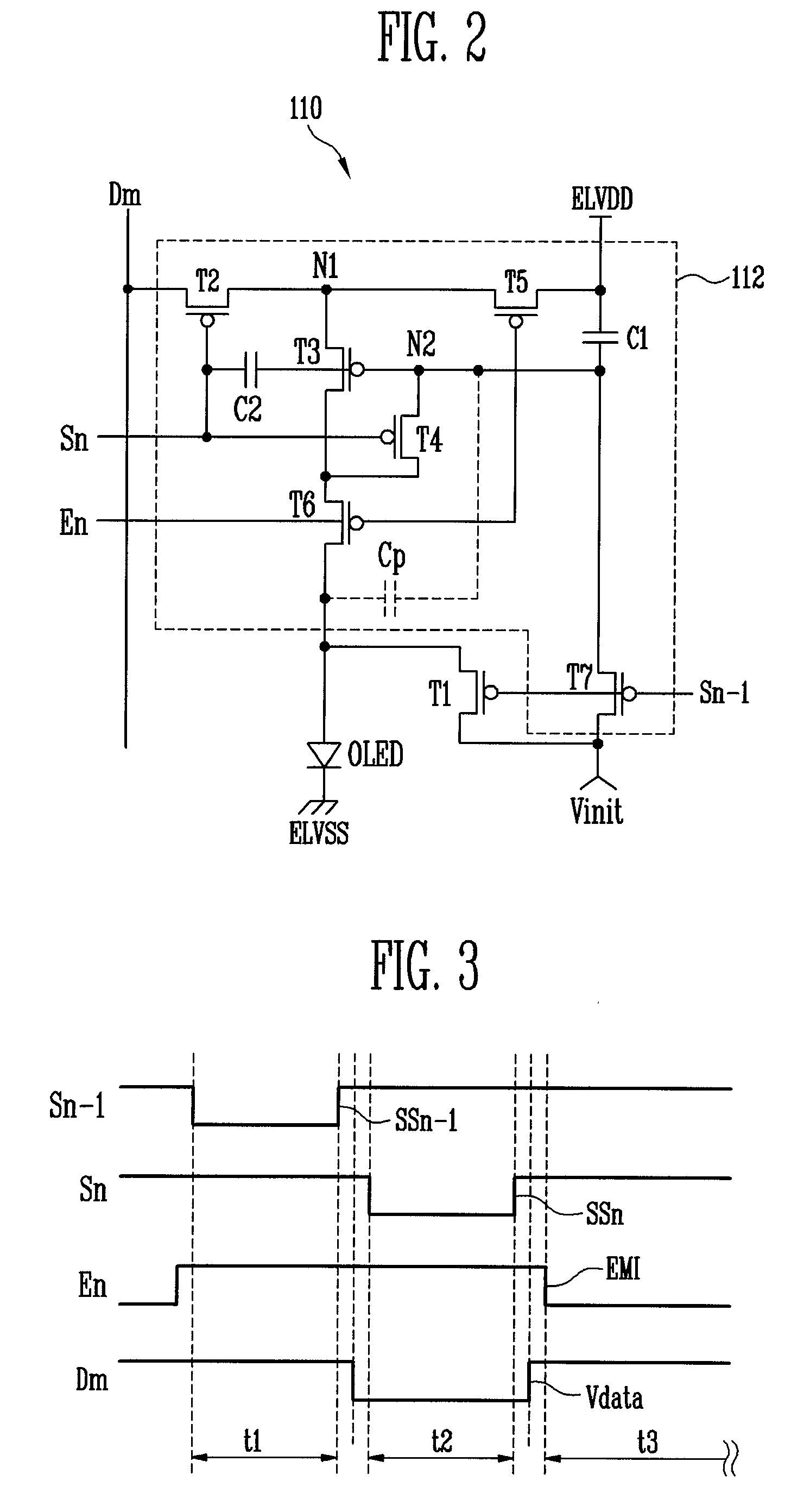
[0020]In a pixel and an organic light emitting display device using the same according to the embodiments of the present invention, each pixel has a reset transistor (e.g., a first transistor) for applying a constant voltage to an anode electrode of an organic light emitting diode during an initialization period. Accordingly, the value of a kickback voltage is maintained constant for each gray level, regardless of the gray level displayed in a previous frame, so that response characteristics of the pixel can be improved, and an image having a uniform image quality can be displayed.

Problems solved by technology

However, response characteristics of a pixel of the AMOLED may be adversely affected by parasitic capacitance generated due to the structure of the pixel, therefore, image quality of an image displayed by a plurality of such pixels may be uneven among the pixels.
Therefore, response characteristics of a pixel may be worsened, and image quality of an image displayed may be degraded.

Method used


Image

  • Pixel and organic light emitting display device using the same
  • Pixel and organic light emitting display device using the same
  • Pixel and organic light emitting display device using the same

Examples


Embodiment Construction

[0026]Hereinafter, certain exemplary embodiments according to the present invention will be described with reference to the accompanying drawings. Here, when a first element is described as being coupled to a second element, the first element may be directly coupled to the second element or indirectly coupled to the second element via a third element. Further, some of the elements that are not essential to a complete understanding of the present invention are omitted for clarity. Also, like reference numerals refer to like elements throughout.

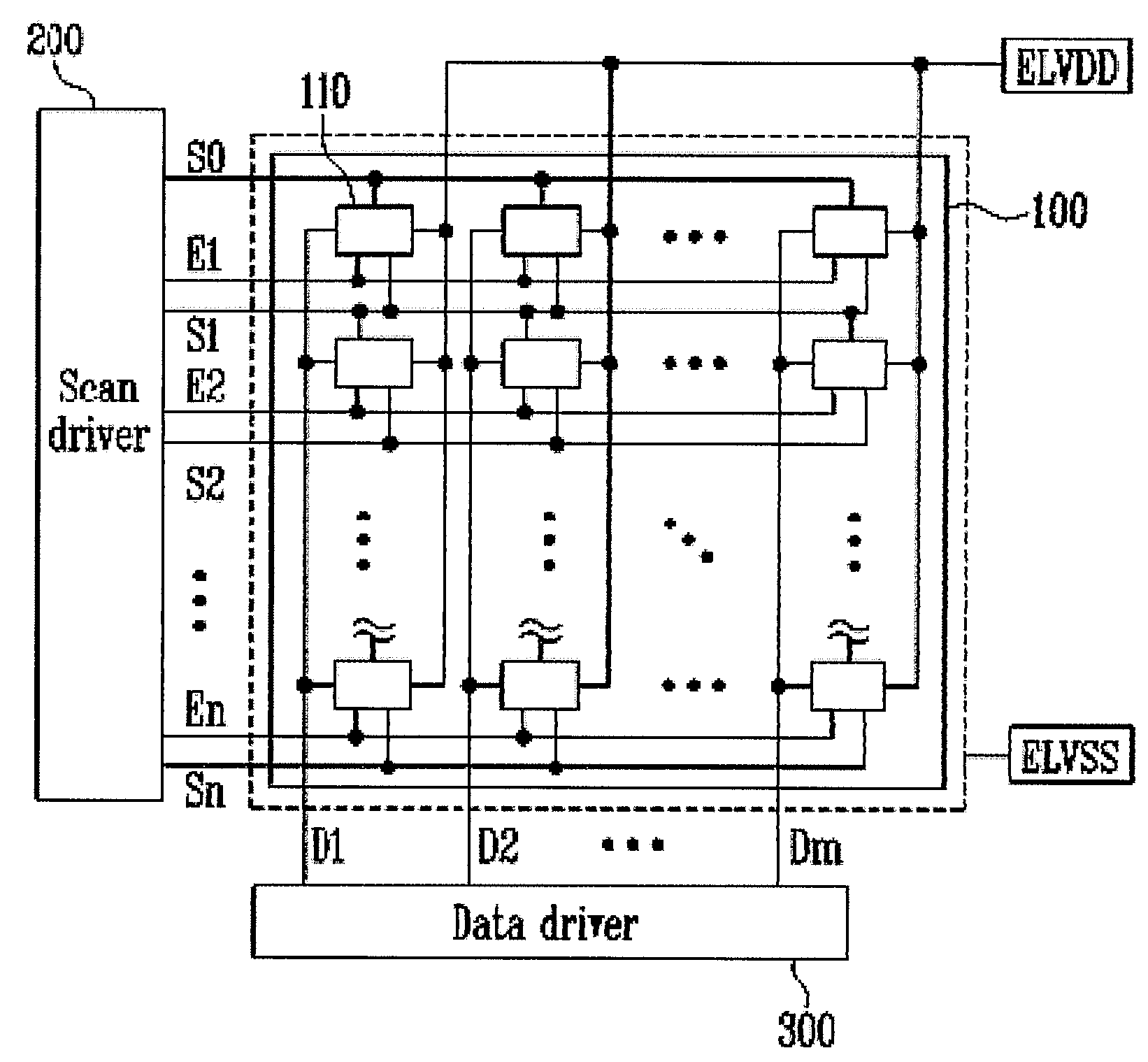
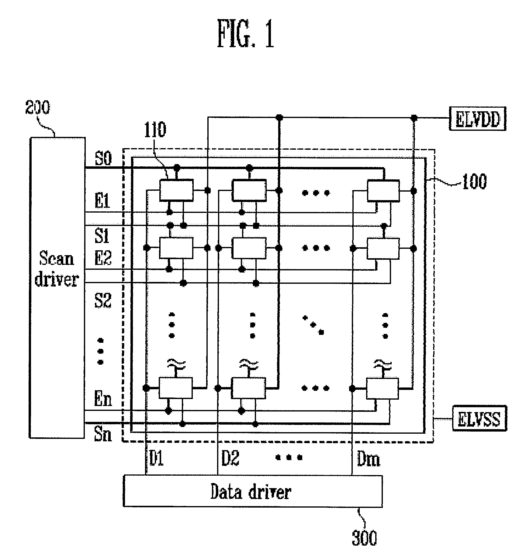
[0027]FIG. 1 is a block diagram schematically showing the configuration of an organic light emitting display device according to an embodiment of the present invention.

[0028]Referring to FIG. 1, the organic light emitting display device according to the embodiment of the present invention includes a display unit 100, a scan driver 200, and a data driver 300.

[0029]The display unit 100 includes a plurality of pixels 110 arranged in a matrix at cr...


PUM


Abstract

A pixel capable of improving response characteristics and displaying an image having a uniform image quality, and an organic light emitting display device using the same. The pixel includes an organic light emitting diode coupled between first power and second power; a pixel circuit coupled between the first power and the organic light emitting diode for supplying a driving current to the organic light emitting diode; and a first transistor for supplying a reset voltage to an anode electrode of the organic light emitting diode during a first period when a previous scan signal is supplied to a previous scan line.

Description

CROSS-REFERENCE TO RELATED APPLICATIONS[0001]This application claims priority to and the benefit of Korean Patent Application No. 10-2008-0070002, filed on Jul. 18, 2008, in the Korean Intellectual Property Office, the entire content of which is incorporated herein by reference.BACKGROUND OF THE INVENTION[0002]1. Field of the Invention[0003]The present invention relates to a pixel and an organic light emitting display device using the same, and more particularly, to a pixel capable of improving response characteristics and displaying an image having a uniform image quality, and an organic light emitting display device using the same.[0004]2. Description of Related Art[0005]Recently, there have been developed various types of flat panel display devices having lighter weight and smaller volume than those of cathode ray tube display devices.[0006]Among these flat panel display devices, an organic light emitting display device displays images by using organic light emitting diodes (OLED...

Claims


Application Information

Patent Timeline
IPC IPC(8): G09G5/00G09G3/30
CPCG09G3/3233G09G2300/0819G09G2310/0251G09G2300/0861G09G2310/0248G09G2300/0852H01L2924/12044
Inventor KWAK, WON-KYU
Owner SAMSUNG DISPLAY CO LTD
Learn More