Method of forming finned semiconductor devices with trench isolation

Active Publication Date: 2010-01-21
INNOVATIVE FOUNDRY TECH LLC
View PDF8 Cites 140 Cited by
  • Summary
  • Abstract
  • Description
  • Claims
  • Application Information

AI Technical Summary

Benefits of technology

[0008]This summary is provided to introduce a selection of concepts in a simplified form that are further described below in the detailed description. This summary is not inten

Problems solved by technology

The cost and complexity of such multiple photolithography and etching steps c

Method used


Image

  • Method of forming finned semiconductor devices with trench isolation
  • Method of forming finned semiconductor devices with trench isolation
  • Method of forming finned semiconductor devices with trench isolation

Examples


Embodiment Construction

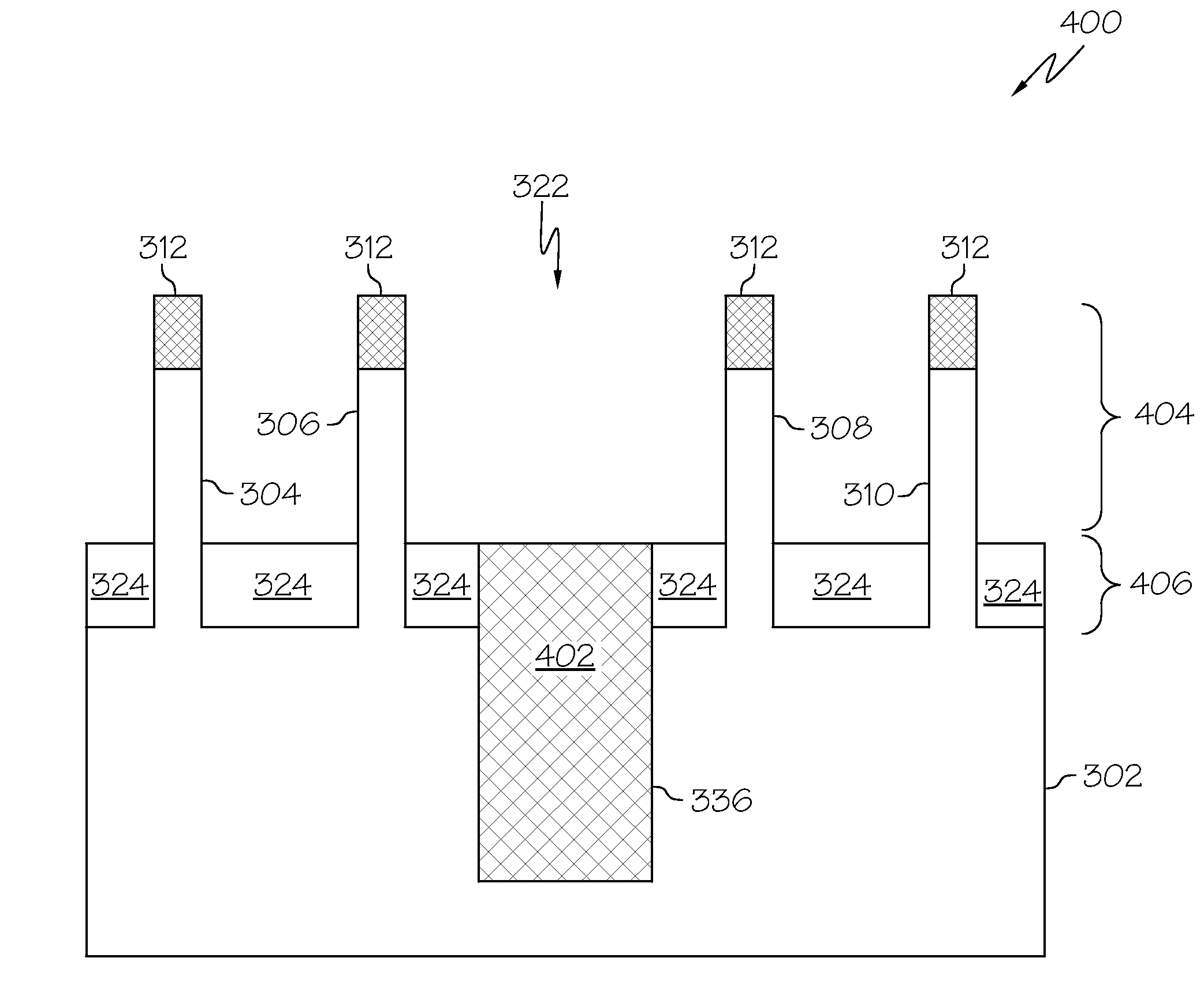
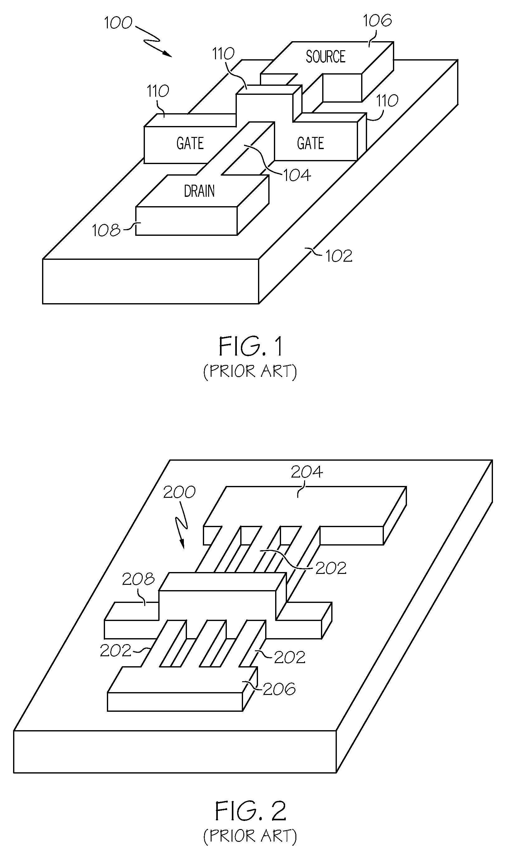
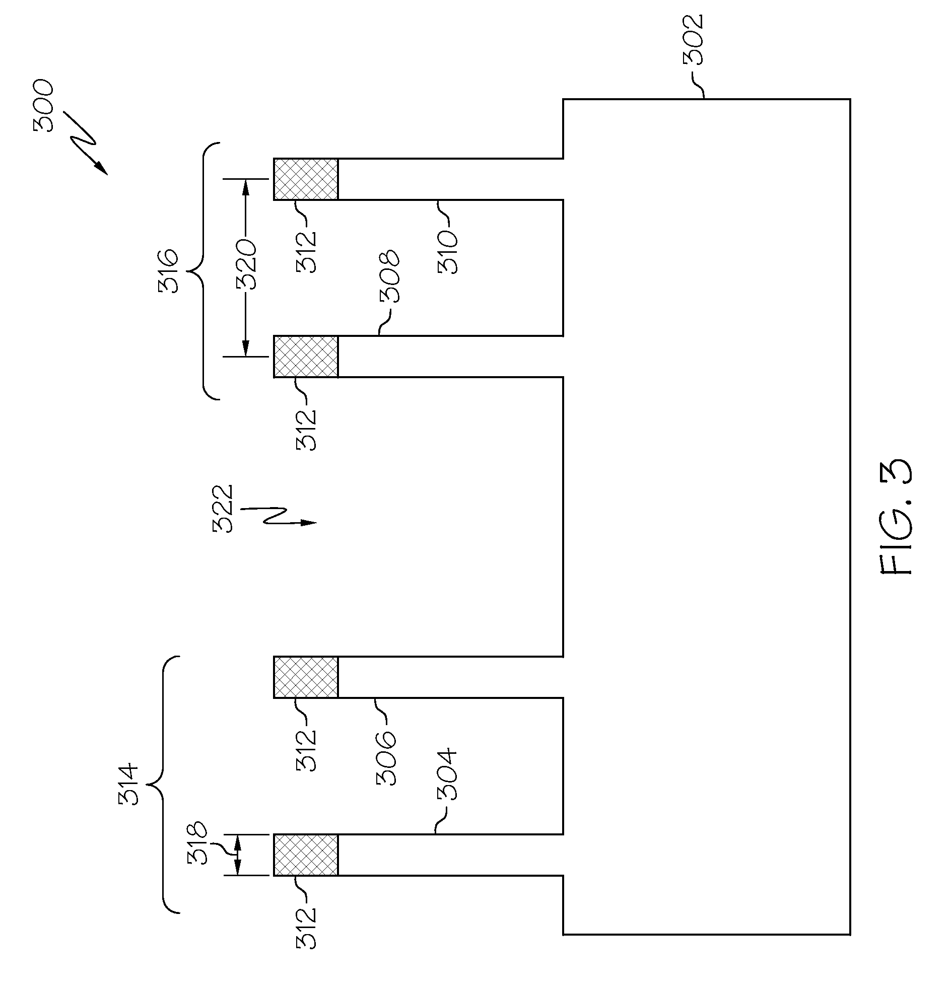
[0014]The following detailed description is merely illustrative in nature and is not intended to limit the embodiments of the subject matter or the application and uses of such embodiments. As used herein, the word “exemplary” means “serving as an example, instance, or illustration.” Any implementation described herein as exemplary is not necessarily to be construed as preferred or advantageous over other implementations. Furthermore, there is no intention to be bound by any expressed or implied theory presented in the preceding technical field, background, brief summary or the following detailed description.

[0015]For the sake of brevity, conventional techniques related to semiconductor device fabrication may not be described in detail herein. Moreover, the various tasks and process steps described herein may be incorporated into a more comprehensive procedure or process having additional steps or functionality not described in detail herein. In particular, various steps in the manu...


PUM


Abstract

A method of manufacturing a semiconductor device structure, such as a FinFET device structure, is provided. The method begins by providing a substrate comprising a bulk semiconductor material, a first conductive fin structure formed from the bulk semiconductor material, and a second conductive fin structure formed from the bulk semiconductor material. The first conductive fin structure and the second conductive fin structure are separated by a gap. Next, spacers are formed in the gap and adjacent to the first conductive fin structure and the second conductive fin structure. Thereafter, an etching step etches the bulk semiconductor material, using the spacers as an etch mask, to form an isolation trench in the bulk semiconductor material. A dielectric material is formed in the isolation trench, over the spacers, over the first conductive fin structure, and over the second conductive fin structure. Thereafter, at least a portion of the dielectric material and at least a portion of the spacers are etched away to expose an upper section of the first conductive fin structure and an upper section of the second conductive fin structure, while preserving the dielectric material in the isolation trench. Following these steps, the fabrication of the devices is completed in a conventional manner.

Description

TECHNICAL FIELD[0001]Embodiments of the subject matter described herein relate generally to semiconductor devices and related manufacturing processes. More particularly, embodiments of the subject matter relate to methods of forming semiconductor devices, such as FinFET devices, having trench isolation.BACKGROUND[0002]Transistors, such as metal oxide semiconductor field-effect transistors (MOSFETs), are the core building block of the vast majority of semiconductor devices. Some semiconductor devices, such as high performance processor devices, can include millions of transistors. For such devices, decreasing transistors size, and thus increasing transistor density, has traditionally been a high priority in the semiconductor manufacturing industry.[0003]A FinFET is a type of transistor that can be fabricated using very small scale processes. FIG. 1 is a simplified perspective view of a FinFET 100, which is formed on a semiconductor wafer substrate 102. A FinFET is named for its use o...

Claims


Application Information

Patent Timeline
IPC IPC(8): H01L21/76
CPCH01L21/76232H01L21/823431H01L29/7851H01L29/66818H01L29/66795H01L29/785
Inventor LIN, MING-RENKRIVOKAPIC, ZORANMASZARA, WITEK
Owner INNOVATIVE FOUNDRY TECH LLC
Why Eureka
Try Eureka