Memory-based fft/ifft processor and design method for general sized memory-based fft processor

Inactive Publication Date: 2010-01-21
NATIONAL CHIAO TUNG UNIVERSITY
11 Cites 12 Cited by

AI-Extracted Technical Summary

Problems solved by technology

(1) [A1] could not support the multi-bank memory structure.
This would result in the FFT needs more computation cycle and thus demand higher clock rate for the processor for real-time application.
(3) [A3] could only support the fixed radix-r, hence, it could not support the Chinese DTV or PLC etc application.
Besides, since it could not support multi-bank memory structu...

Method used

[0034]Since the input data of each 4-point FFT has the same index ñ2, memory conflict could be avoided in the first stage by distributing the data into different memory banks by Eq. (7).
[0050]Table II is the comparison of this invention between different approaches for the real-time application for the memory-based DFT processor design. For [B4], it needs 4N words memory size and is two times of the others. This is because it doesn't adopt the in-place policy fo...

Benefits of technology

[0016]To overcome the drawbacks of the prior arts, this invention proposes a design method of general sized memory-based FFT processor, comprising the steps of: (1) Decomposing a large size FFT computation into several relative smaller sizes FFT by decomposition equation and then transform the original index from one dimension into multi-dimension vector; (2) Controlling the index vector to distribute the input data into different memory banks such that both the in-place policy for computation and the multi-bank memory for high-radix structure could be supported simultaneously without memory conflict; (3...

Abstract

For a large size FFT computation, this invention decomposes it into several smaller sizes FFT by decomposition equation and then transform the original index from one dimension into multi-dimension vector. By controlling the index vector, this invention could distribute the input data into different memory banks such that both the in-place policy for computation and the multi-bank memory for high-radix structure could be supported simultaneously without memory conflict. Besides, in order to keep memory conflict-free when the in-place policy is also adopted for I/O data, this invention reverses the decompose order of FFT to satisfy the vector reverse behavior. This invention can minimize the area and reduce the necessary clock rate effectively for general sized memory-based FFT processor design.

Application Domain

Digital computer detailsComplex mathematical operations

Technology Topic

DecompositionMultiple dimension +8

Image

  • Memory-based fft/ifft processor and design method for general sized memory-based fft processor
  • Memory-based fft/ifft processor and design method for general sized memory-based fft processor
  • Memory-based fft/ifft processor and design method for general sized memory-based fft processor

Examples

  • Experimental program(1)

Example

[0019]For the best understanding of this invention, please refer to the following detailed description of the preferred embodiments and the accompanying drawings.
[0020]The definition of DFT is
X ( k ) = ∑ n = 0 N - 1 x ( n ) W N nk .
The method to decompose a larger size DFT into several smaller sizes DFT has been proposed in article C1 [C. Burrus, “Index mappings for multidimensional formulation of the DFT and convolution,”IEEE Trans. Acoust., Speech, Signal Process., vol. 25, no. 3, pp. 239-242, June 1977]. Here, the present invention takes the decomposition equation (1) for the size N=N1N2 for illustration:
{ n = N 2 n 1 + A 2 n 2 mod N n 1 , k 1 = 0 , 1 , … , N 1 - 1 k = B 1 k 1 + N 1 k 2 mod N n 2 , k 2 = 0 , 1 , … , N 2 - 1 ( 1 )
[0021]Eq. (1) maps the index n and k to the index vector (n1, n2) and (k1, k2), from one dimension [0, N−1] into two dimensions [0, N1−1]×[0, N2−1]. The selection of coefficient A2 and B1 depends on the relation between N1 and N2. In this invention, the coefficients for Eq. (1) are employed as follows:
[0022]Case I: If N1 and N2 are relative prime, we choose A2 and B1 such that
A2=p1N1 and A2=q1N2+1
B1=P2N2 and B1=q2N1+1
[0023]Here, p1, q1, p2 and q2 are all positive integers. Then, the definition of DFT could be rewritten as Eq. (2):
X ( k 1 , k 2 ) = ∑ n 2 ∑ n 1 x ( n 1 , n 2 ) W N 1 n 1 k 1 W N 2 n 2 k 2 = ∑ n 2 { ∑ n 1 x ( n 1 , n 2 ) W N 1 n 1 k 1 } W N 2 n 2 k 2 = ∑ n 2 y ( k 1 , n 2 ) W N 2 n 2 k 2 ( 2 )
[0024]Case II: If N1 and N2 are not relative prime, we choose A2=B1=1. Then, the definition of DFT could be rewritten as Eq. (3):
X ( k 1 , k 2 ) = ∑ n 2 ∑ n 1 x ( n 1 , n 2 ) W N 1 n 1 k 1 W N 2 n 2 k 2 W N n 2 k 1 = ∑ n 2 { W N n 2 k 1 ∑ n 1 x ( n 1 , n 2 ) W N 1 n 1 k 1 } W N 2 n 2 k 2 = ∑ n 2 W N n 2 k 1 y ( k 1 , n 2 ) W N 2 n 2 k 2 ( 3 )
[0025]Eqs. (2) and (3) imply that a larger size N-point FFT could be computed by two smaller sized N1-point and N2-point FFT in the first and second stages respectively. For the fixed n2, the input data of the N1-point FFT in the first stage are x(n1, n2), n1=0, 1, . . . , N1−1. The output data of the first stage correspond to this n2 are y(k1, n2), k1=0, 1, . . . , N1−1. For the fixed k1, the input data of the N2-point FFT in the second stage are y(k1, n2), n2=0, 1, . . . , N2−1. The output data of the second stage correspond to this k1 are X(k1, k2), k2=0, 1, . . . , N2−1. The difference between Eq. (2) and (3) is that if N1 and N2 are not relative prime, there would have twiddle factor wNn 2 k 1 between the first and second stages as shown in Eq. (3).
[0026]Now, the present invention considers computing N1-point DFT in the first stage and N2-point DFT in the second stage for the first DFT symbol. The present invention distributes the input data into different memory banks. Suppose N2≧N1 and the memory bank number is N2, then, the input data could be distributed into N2 memory banks by Eq. (4) to achieve memory conflict-free.
bank=n1+n2 mod N2 (4)
[0027]The key to achieve memory conflict-free is to distribute data into memory bank by Eqs. (1) and (4). Once the memory bank is selected, data need to be addressed. Any two data in the same memory bank should be mapped to different address within the range from 0 to N1−1. For simplicity, we choose Eq. (5) for data addressing.
address=n1 (5)
[0028]After finishing computing the first DFT symbol, the data should be outputted in order. The output index is mapped by Eq. (4). When the computed DFT symbol data are outputted in order, the input data of the second DFT symbol are also inputted in order simultaneously with the in-place policy. That is, the new input data x(i) should be put in the location of the output data y(i). For the computation of the second DFT symbol, the present invention computes it with the reverse order of the first DFT symbol. The present invention computes the N2-point DFT in the first stage and N1-point DFT in the second stage for the second DFT symbol. After finishing computing the second DFT symbol, the I/O data also adopts the in-place policy. The third DFT symbol would return to the state of the first DFT symbol.
[0029]The following, the present invention takes the 3780-point FFT as example for detailed illustration, which has been adopted for the Chinese DTV application. The decomposition order in following is only one of the candidate selections.
[0030]Since 3780=4×3×3×3×5×7, we could complete it by computing the 3-point, 4-point, 5-point and 7-point FFT respectively. Here, the data are distributed into 7 memory banks.
[0031]First, the present invention takes the decomposition order, 4, 3, 3, 3, 5 and then 7. For the first stage (4-point FFT), the decomposition equation (6) is taken.
{ n = 945 n 1 + 2836 n ~ 2 mod 3780 n 1 , k 1 = 0 , 1 , 2 , 3 k = 945 k 1 + 4 k ~ 2 mod 3780 n ~ 2 , k ~ 2 = 0 , … , 944 ( 6 )
[0032]It maps the index n to the vector (n1,ñ2) from [0, 3779] to [0, 3]×[0, 944] as shown in Table I
TABLE I THE INDEX MAPPING FOR THE FIRST STAGE n1 = 0 n1 = 1 n1 = 2 n1 = 3 ñ2 = 0 x[0] x[945] x[1890] x[2835] ñ2 = 1 x[2836] x[1] x[946] x[1891] ñ2 = 2 x[1892] x[2837] x[2] x[947] . . . . . . . . . . . . . . . ñ2 = 944 x[944] x[1889] x[2834] x[3779]
[0033]The data in each row of Table I are the input data of each 4-point FFT The input order is decided by the index n1. For example, for the row ñ2=1, the input order is (n1, ñ2 )=(0,1), (1,1), (2,1) and (3,1). They correspond to the data x[2836], x[1], x[946] and x[1891] respectively as shown in Table I.
[0034]Since the input data of each 4-point FFT has the same index ñ2, memory conflict could be avoided in the first stage by distributing the data into different memory banks by Eq. (7).
bank=n1+×mod7   (7)
[0035]After the first stage, the original data has been divided into 4 independent groups for four 945-point FFT and correspond to k1=0, 1, 2 and 3 respectively.
[0036]Similarly, for the 945-point FFT, we could also decompose it in the order 945=3×3×3×5×7 and map the index ñ2 to the vector (n2, n3, n4, n5, n6) from [0, 944] to [0, 2]×[0, 2]×[0, 2]×[0, 4]×[0, 6]. By combining all the decomposition equations for each stage, the full index mapping equations for the 3780-point FFT in this decomposition order are shown in Eqs. (8) and (9). The bank selection Eq. (10) is taken for memory conflict-free. And, the addressing equation could be taken as Eq. (11).
n=945n1+1260n2+2940n3+980n4+1512n5+540n6 mod3780   (8)
k=945k1+2380k2+3360k3+2520k4+2268k5+540k6 mod3780   (9)
bank=n1+n2+n3+n4+n5+n6 mod7   (10)
address=135n1+45n2+15n3+5n4+n5 (11)
[0037]After the first FFT symbol, the odd FFT symbol, has been computed, all the indexes ni would be transformed to ki in Eqs. (10) and (11). For the second input FFT symbol, the even FFT symbol, since the even FFT input data xeven[n] should be put in the location of the odd FFT output data xodd[k] with k=n, its mapping index, memory bank and address should be determined by Eqs. (9), (10) and (11) respectively.
[0038]Now, the present invention considers how to keep memory conflict-free under this data distribution for the even FFT symbol.
[0039]For the computation of the even FFT symbol, the present invention takes the reverse decomposition order of the odd FFT symbol, 3780=7×5×3×3×3×4. That is, the present invention computes it in the order 7-point, 5-point, 3-point, 3-point, 3-point and 4-point FFT. By the similar approach, the present invention could get the full input and output index mapping Eqs. (12) and (13) for the even FFT symbols just like Eqs. (8) and (9) for the odd FFT symbols. They map the input index n and output index k to the vector (a1, a2, a3, a4, a5, a6) and (b1, b2, b3, b4, b5, b6) respectively from [0, 3779] to [0, 6]×[0, 4]×[0, 2]×[0, 2]×[0, 2]×[0, 3] for the even FFT symbols.
n=540a1+2268a2+2520a3+3360a4+2380a5+945a6 mod3780   (12)
k=540b1+1512b2+980b3+2940b4+1260b5+945b6 mod3780   (13)
[0040]Comparing the input and output index mapping equation pair (9) with (12) and (8) with (13), the present invention finds that these two equation pairs could match perfectly with the relation, vector reverse, as shown in Eqs. (14) and (15).
(a1, a2, a3, a4, a5, a6)=(k6, k5, k4, k3, k2, k1)   (14)
(n1, n2, n3, n4, n5, n6)=(b6, b5, b4, b3, b2, b1)   (15)
[0041]Since the input data of the even FFT symbol xeven[n] should be put in the location of the odd computed FFT symbol output data Xodd[k] with k=n. Then, the present invention gets Eqs. (16) and (17) for bank selection and memory addressing for the even FFT symbol.
bank=a1+a2+a3+a4+a5+a6 mod7   (16)
address=135a6+45a5+15a4+5a3+a2 (17)
[0042]Note the input mapping equation (12) and the output mapping equation (9) are the same. And, the bank selection equations (10) and (16) also keep the same. Thus the memory access would keep conflict-free for the even FFT symbol by computing it with the reverse decomposition order of the odd FFT symbol.
[0043]Furthermore, the present invention notes that the output mapping equation (13) and the input mapping equation (8) are also the same. This means that, when the third FFT input data xthird[n] is put in the location of the even FFT output data Xeven[k] with k=n, the distribution of the third FFT input data would be the same with that being determined by Eqs. (8), (10) and (11). It returns to the state of the odd FFT symbol and we have xthird[n]=xodd[n].
[0044]From above discussion, a conflict-free variable radix FFT processor could be designed by reversing the decomposition order of the previous FFT symbol. It could support the in-place policy for both butterflies output and I/O data simultaneously.
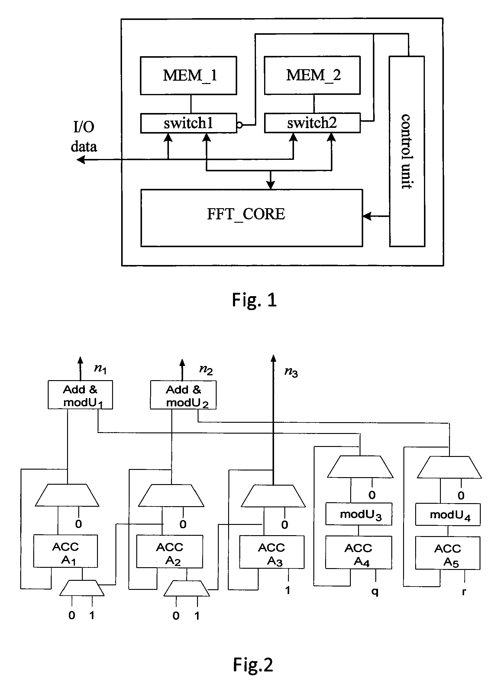
[0045]FIG. 1 shows the memory-based 3780-point DFT processor design block diagram. The MEM_1 and MEM_2 are two memory blocks, each block contains 7 memory banks and each bank has 540 words. The FFT_CORE contains the processing element which could process the smaller sized DFT individually. The control unit controls the data access and processing element computation. The following, the present invention describes how the DFT processor work. For convenience, the present invention denotes the decomposition and computation order as type I order: 4-point, 3-point, 3-point, 3-point, 5-point and then 7-point DFT. And, the present invention denotes the reverse order of type I as type II order: 7-point, 5-point, 3-point, 3-point, 3-point and then 4-point DFT.
[0046]Suppose the 1st and the 2nd DFT symbols are stored in the memory blocks MEM_1 and MEM_2 respectively. And suppose the decomposition and computation order of the 1st and the 2nd DFT symbol are both in the type I order. Then, from the previous discussion, the present invention has:
[0047](1) the 1st, 5th, 6th, 13th, . . . DFT symbols are stored in MEM_1 and computed in type I order.
[0048](2) the 2nd, 6th, 10th, 14th, . . . DFT symbols are stored in MEM_2 and computed in type I order. (3) the 3rd, 7th, 11th, 15th, . . . DFT symbols are stored in MEM_1 and computed in type II order. (4) the 4th, 8th, 12th, 16th, . . . DFT symbols are stored in MEM_2 and computed in type II order.
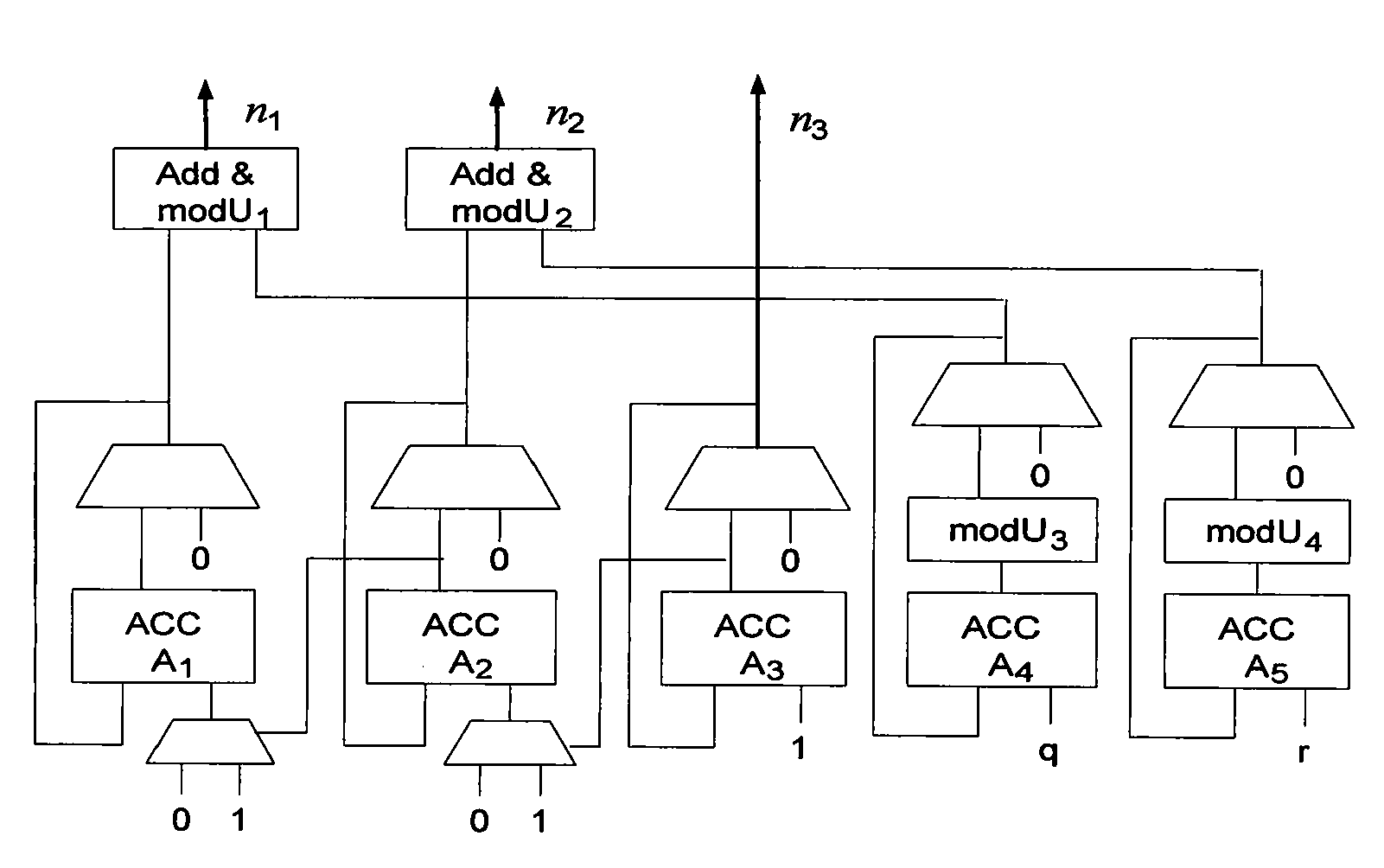
[0049]For convenience, for the hardware implementation to get the index vector for data access, the present invention only shows the implement for the DFT size N=N1N2N3 in FIG. 2. As shown in FIG. 2, it is consists of several accumulators A1, A2, . . . , A5. The parameters U1, U2, U3, U4, q and r are determined by the decomposition equation (1) for each stage.
[0050]Table II is the comparison of this invention between different approaches for the real-time application for the memory-based DFT processor design. For [B4], it needs 4N words memory size and is two times of the others. This is because it doesn't adopt the in-place policy for butterflies computation and I/O data. Hence, in order to minimize the necessary memory size, the in-place policy should be adopted for both butterflies computation and I/O data. Exclusive of [B4], all of the others, only this invention and [A1] can support the mixed of any general radix and then for any size FFT. However, [A1] could not support the multi-bank memory structure without memory conflict to reduce the necessary clock rate for real-time application.
[0051]In this invention, the inventors propose the approach for memory based FFT processor design such that it could support the following three items simultaneously: (1) the in-place policy for both butterflies computation and I/O data (2) the mixed of any radix (3) the multi-bank memory structure.
TABLE II THE COMPARISON BETWEEN DIFFERENT APPROACH [A1] [A2] [B2] [A5] [A3] [A4] B[3] This invention Radix All general Fixed radix-r Fixed radix-r Radix-2/4 All general In-place Yes Yes Yes Yes Yes Memory 2N words 2N words 2N words 2N words 2N words Multi-bank No Yes No Yes Yes
[0052]When this invention apply the proposed for the 3780-point DFT in Chinese DTV application, this invention could use only 2N words memory to achieve the system requirement, continuous data flow and in order I/O data. However, in order to achieve this, the solution [A6]-[A8] needs at least 3N words, [A9], [A11] needs at least 5N wo [A10] needs 6N words, and [B1] needs more than 3N words. Hence, for this application, if the 3780-point DFT processor is designed with this invention, the chip area could be reduced significantly than the processor which is designed with any current solution.
[0053]Although a preferred embodiment of the invention has been described for purposes of illustration, it is understood that various changes and modifications to the described embodiment can be carried out without departing from the scope of the invention as disclosed in the appended claims.

PUM

no PUM

Description & Claims & Application Information

We can also present the details of the Description, Claims and Application information to help users get a comprehensive understanding of the technical details of the patent, such as background art, summary of invention, brief description of drawings, description of embodiments, and other original content. On the other hand, users can also determine the specific scope of protection of the technology through the list of claims; as well as understand the changes in the life cycle of the technology with the presentation of the patent timeline. Login to view more.

Similar technology patents

Plasma display panel for multi-screen and fabricating method for the same

InactiveUS20100072871A1ensure continuityminimize area
Owner:ORION CORP

Classification and recommendation of technical efficacy words

Why Eureka
Try Eureka