Active matrix array device

a technology of active matrix array and array device, which is applied in the direction of static indicating device, instruments, etc., can solve the problems of reducing the aperture of the pixel and the amount of light that can be transmitted, and achieve the effect of better us

Inactive Publication Date: 2010-01-28
KONINKLIJKE PHILIPS ELECTRONICS NV
View PDF6 Cites 5 Cited by
  • Summary
  • Abstract
  • Description
  • Claims
  • Application Information

AI Technical Summary

Benefits of technology

[0012]In one embodiment, a shorting transistor is provided across the gain element, and the input of the gain element is connected to the addressing switch o...

Problems solved by technology

However, the storage capacitors are normally formed using at least one opaque layer so that increasing the area of the sto...

Method used


Image

  • Active matrix array device
  • Active matrix array device
  • Active matrix array device

Examples


Embodiment Construction

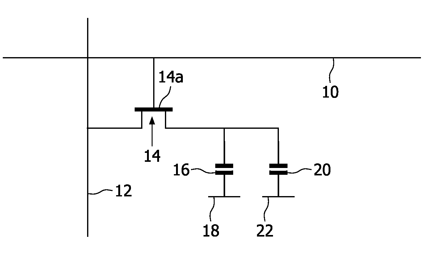
[0025]FIG. 1 shows a conventional pixel configuration for an active matrix liquid crystal display. The display is arranged as an array of pixels in rows and columns. Each row of pixels shares a common row conductor 10, and each column of pixels shares a common column conductor 12. Each pixel comprises a thin film transistor 14 and a liquid crystal cell 16 arranged in series between the column conductor 12 and a common electrode 18. The transistor 14 is switched on and off by a signal provided on the row conductor 10. The row conductor 10 is thus connected to the gate 14a of each transistor 14 of the associated row of pixels. Each pixel additionally comprises a storage capacitor 20 which is connected at one end 22 to the next row electrode, to the preceding row electrode, or to a separate capacitor electrode. This capacitor 20 stores a drive voltage so that a signal is maintained across the liquid crystal cell 16 even after the transistor 14 has been turned off.

[0026]In order to driv...


PUM


Abstract

An active matrix array device comprises an array of device elements, each device element having an associated circuit. Each circuit comprises an addressing switch (14) and a storage capacitor (20) for maintaining a voltage applied to the device element (16) through the addressing switch (14). Each circuit is associated with a gain element (36), and the storage capacitor (20) is in a feedback path of the gain element. The gain element (36) is used as a way to increase the effective value of the storage capacitor, so as to provide an improvement in the performance of active matrix devices.

Description

FIELD OF THE INVENTION[0001]The invention relates to an active matrix array device, for example an active matrix display.BACKGROUND OF THE INVENTION[0002]Active matrix array devices often use capacitors within the array elements of the device in order to temporarily store information. For example, in the case of a liquid-crystal display (LCD), the voltage required to set the brightness of each display pixel is stored on the capacitance of the pixel. This capacitance typically consists of the capacitance of the liquid crystal cell and an additional storage capacitor. The storage capacitor increases the total capacitance of the pixel and improves the operation of the display, for example by reducing the effect of leakage currents within the transistors of the active matrix array.[0003]The performance of an active matrix display such as an LCD is generally improved by increasing the value of the storage capacitance within each pixel. However, the storage capacitors are normally formed ...

Claims


Application Information

Patent Timeline
IPC IPC(8): G09G3/36G09G3/20
CPCG09G3/3648G09G2300/0465G09G2320/0214G09G2300/0819G09G2300/0833G09G2300/0809
Inventor EDWARDS, MARTINAYRES, JOHN RICHARD ALAN
Owner KONINKLIJKE PHILIPS ELECTRONICS NV
Why Eureka
Try Eureka