

Capacitance Structures for Defeating Microchip Tampering
a technology of capacitors and microchips, applied in the field of microchip technology, can solve the problems of obstructing the insertion of ions and electrons, the obstructing of photon observation, and the inability to integrate protective measures within the microchip to hinder reverse engineering techniques,
- Summary
- Abstract
- Description
- Claims
- Application Information
AI Technical Summary
Benefits of technology
Problems solved by technology
Method used
Image

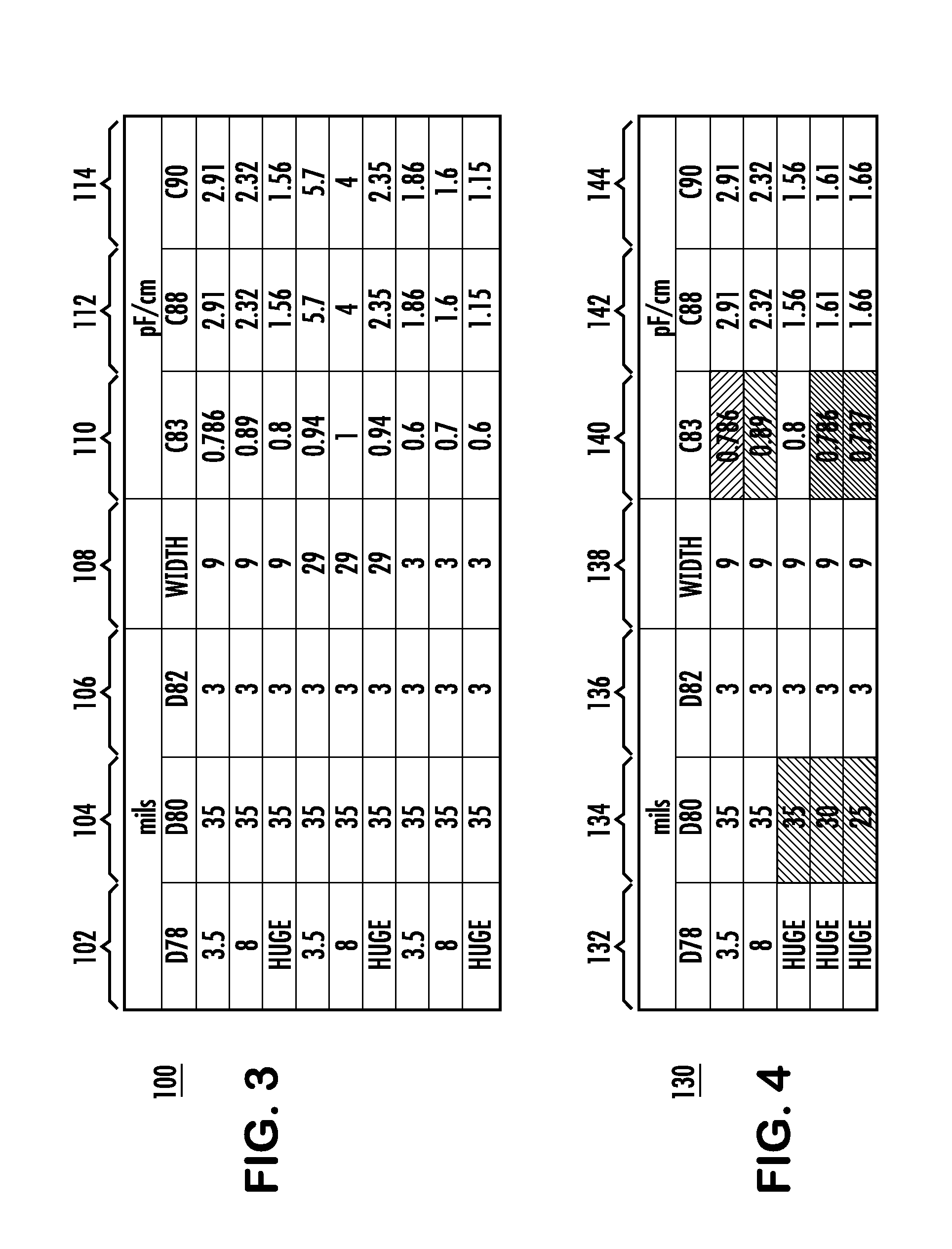
Examples
Embodiment Construction
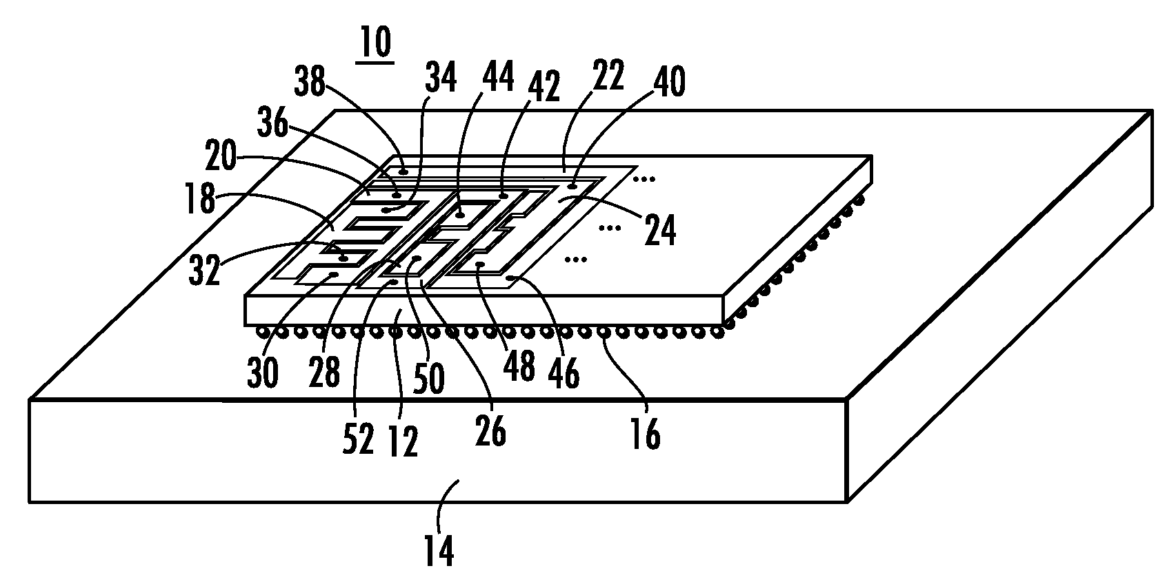
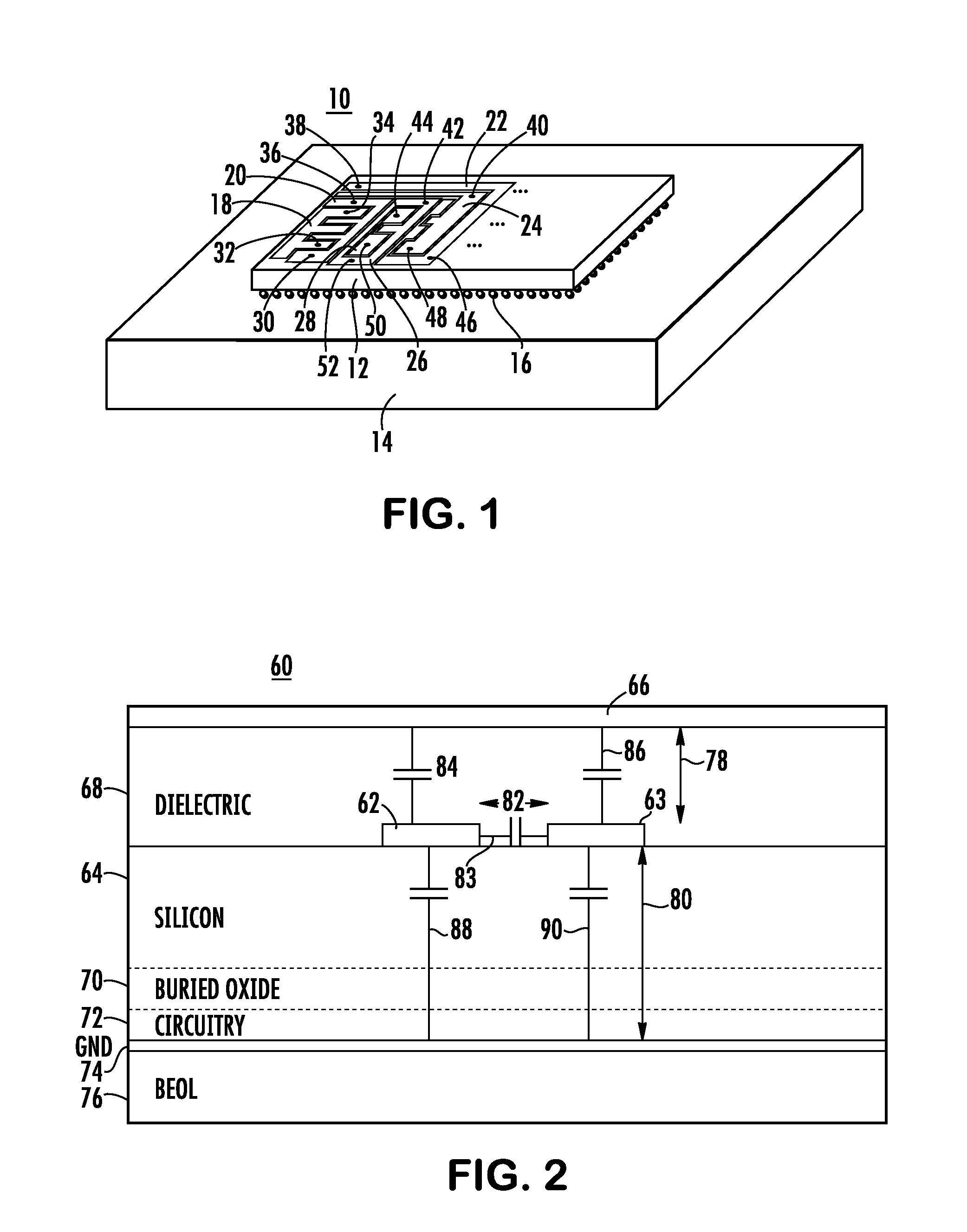
[0024]Embodiments consistent with the underlying principles of the present invention may detect an attempt to tamper with a microchip by detecting an unacceptable alteration in a measured capacitance associated with capacitance structures proximate the backside of a microchip. The capacitance structures typically comprise metallic shapes and may connect using through-silicon vias to active sensing circuitry within the microchip. In response to the sensed change, a shutdown, spoofing, self-destruct or other defensive action may be initiated to protect security sensitive circuitry of the microchip.
[0025]Aspects of the invention may include a plurality of coplanar capacitance structures that are formed by adding copper or another metal to the backside of a microchip die. Through-silicon vias or other connections may connect each capacitance structure to sensing circuitry. The sensing circuitry may be used to determine if the proper capacitance is present.
[0026]More particularly, an imp...
PUM
 Abstract
Description
Claims
Application Information