Printed wiring board and connection configuration of the same

a technology of printed wiring and connection configuration, which is applied in the direction of printed circuit manufacturing, printed circuit aspects, electrical apparatus construction details, etc., can solve the problems of further reducing the area and hinder the further reduction of the area, so as to prevent solder bridging and reduce the wiring pitch

Inactive Publication Date: 2010-02-04
FUJIKURA LTD
View PDF43 Cites 3 Cited by
  • Summary
  • Abstract
  • Description
  • Claims
  • Application Information

AI Technical Summary

Benefits of technology

[0011]On the other hand, there is required in a substrate connecting technology an area saving of a connection portion due to a demand for miniaturization of an electric appliance, in addition to an enhancement of the connection strength between the substrates. The connection configurations disclosed in the above publications emphasize a narrower wire width formed on one of the two substrates to be connected, mainly in view of promoting a fillet and enhancing the connection strength between the wiring pattern and the film base material. Although it is possible to make a wire separation narrower within a permissible range for insulation in order to reduce the connection area in such a configuration where a width of the wiring pattern (connection terminal) needs to be reduced, there exists a restriction which hinders further reduction of the area if the other substrate to be connected has a wider wiring pattern (connection terminal portion).
[0012]The present invention has been made in view of the above circumstances and an aspect of the present invention is to provide a printed wiring board that is capable of further reducing a terminal wiring separation in a connection terminal portion and thus preventing short-circuit due to solder bridging, and a connection configuration of the same.

Problems solved by technology

Although it is possible to make a wire separation narrower within a permissible range for insulation in order to reduce the connection area in such a configuration where a width of the wiring pattern (connection terminal) needs to be reduced, there exists a restriction which hinders further reduction of the area if the other substrate to be connected has a wider wiring pattern (connection terminal portion).

Method used


Image

  • Printed wiring board and connection configuration of the same
  • Printed wiring board and connection configuration of the same
  • Printed wiring board and connection configuration of the same

Examples


Embodiment Construction

[0041]Non-limiting, exemplary embodiments of the present invention will now be described with reference to the accompanying drawings. It should be noted that the accompanying drawings, whether alone or thereamong, are not to scale but merely schematic representations and are not intended to portray the specific parameters or structural details of the invention, which should be determined by a person having ordinary skill in the art through the following description herein.

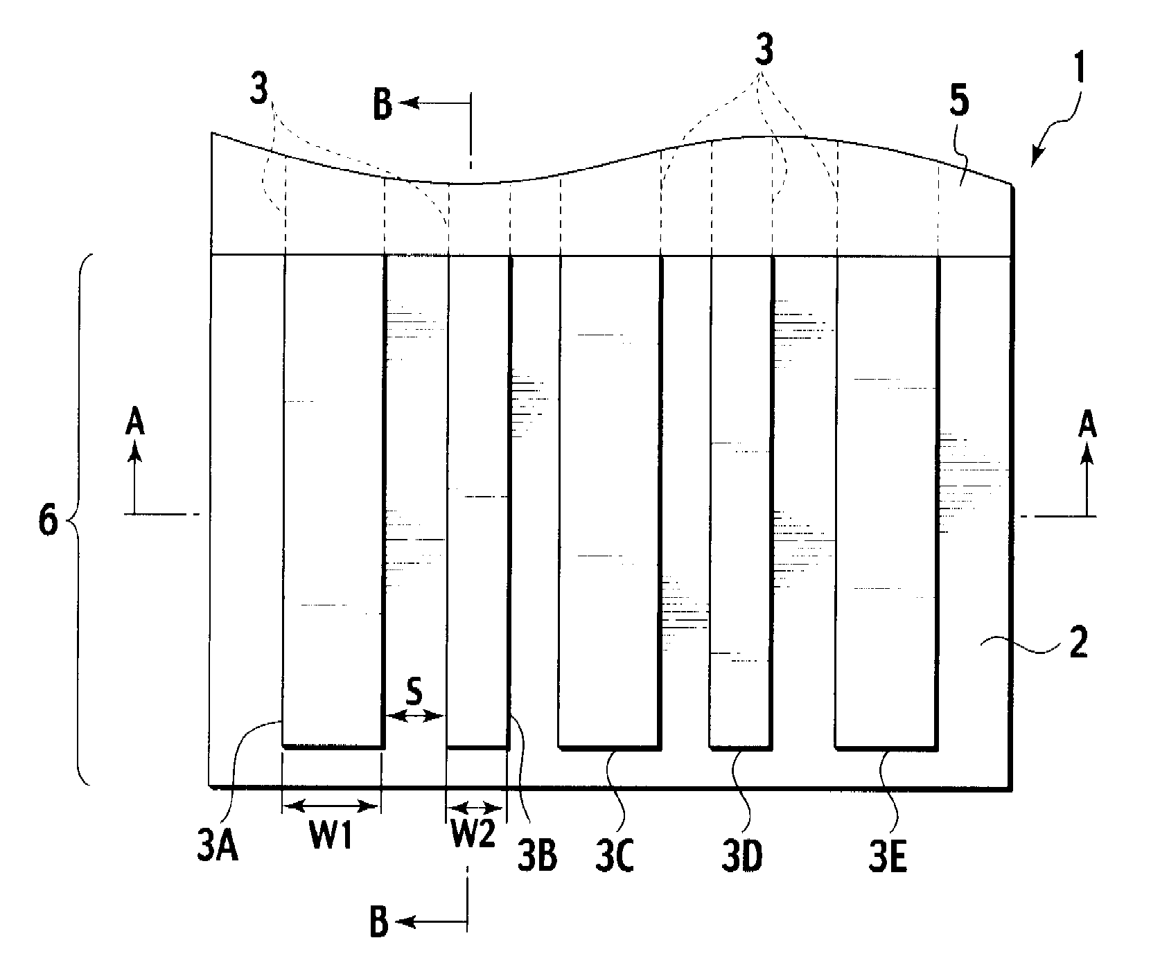
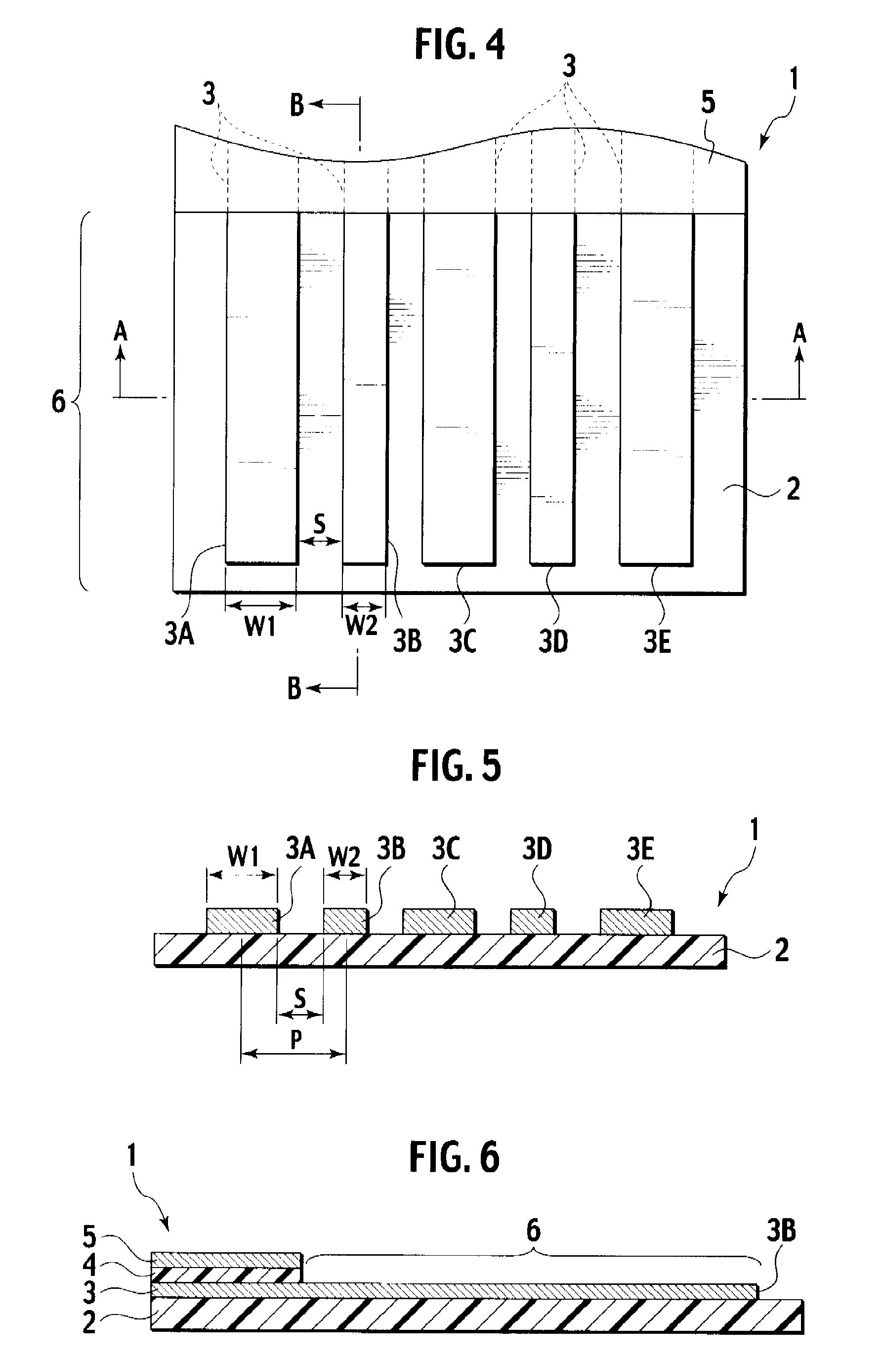
[0042]FIGS. 4 to 5 illustrate a printed wiring board 1 according to a first non-limiting embodiment. Specifically, FIG. 4 is a plan view of a substantial portion of the printed wiring board 1; FIG. 5 is a cross-sectional view taken along a line A-A in FIG. 4; and FIG. 6 is a cross-sectional view taken along a line B-B in FIG. 4.

[0043]The printed wiring board 1 is generally composed of an insulating base material 2, a plurality of wirings 3 formed so as to have a predetermined pattern on at least one surface of the ...


PUM


Abstract

A printed wiring board having an insulating base material; a wiring formed on at least one surface of the insulating base material, the wiring forming a predetermined circuit pattern; a first connection terminal portion formed on the surface and electrically connected to the wiring, the first connection terminal portion having a first width; a second connection terminal portion formed on the surface and electrically connected to the wiring, the second connection terminal portion having a second width; and a cover layer configured to cover the wiring and expose the first and the second connection terminal portion.

Description

[0001]This is a Continuation of application Ser. No. 11 / 676,213 filed Feb. 16, 2007. The entire disclosure of the prior application, application Ser. No. 11 / 676,213 is hereby incorporated by reference. This application claims priority under 35 U.S.C. §119 to Japanese Patent Application No. 2006-040894, filed on Feb. 17, 2006, the entire contents of which are incorporated by reference herein.BACKGROUND[0002]The present invention relates to a printed wiring board for use in various electrical apparatuses and a connection configuration of the same. Specifically, the present invention relates to a printed wiring board including a terminal portion to be connected by use of solder and its connection configuration.DESCRIPTION OF THE RELATED ART[0003]There has been known a soldering connection as one example of a method of connecting a substrate flexible enough to be foldable with a rigid substrate, or connecting two flexible substrates. There will be briefly explained a related-art connect...

Claims


Application Information

Patent Timeline
Patent Type & Authority Applications(United States)
IPC IPC(8): H05K7/00H05K1/09
CPCH05K1/117H05K3/363H05K2201/09727H05K2201/097H05K2201/09427H05K1/02
Inventor KITADA, TOMOFUMIMARUO, HIROKI
Owner FUJIKURA LTD
Why Eureka
Try Eureka