Ldmos device for ESD protection circuit

a protection circuit and metal oxide semiconductor technology, applied in the field of semiconductor devices, can solve the problems of ic chip damage or breakage, esd ldmos device is useless in protecting the output driver, and the semiconductor device and circuit in the ic can be damaged or broken, so as to achieve the effect of turning on more quickly

Active Publication Date: 2010-02-11
UNITED MICROELECTRONICS CORP
View PDF28 Cites 75 Cited by
  • Summary
  • Abstract
  • Description
  • Claims
  • Application Information

AI Technical Summary

Benefits of technology

[0008]The present invention provides a LDNMOS device for an ESD protection circuit. The ESD LDNMOS device can be turned on more quickly than the internal device to be protected.

Problems solved by technology

Semiconductor devices and circuits in ICs can be damaged by ESD.
Thus, the IC chip is damaged or broken by the transient power of ESD.
Thus, the output driver might be turned on more quickly than the LDNMOS device for an ESD protection circuit (ESD LDNMOS device); hence, the ESD LDNMOS device is useless in protecting the output driver.

Method used


Image

  • Ldmos device for ESD protection circuit
  • Ldmos device for ESD protection circuit
  • Ldmos device for ESD protection circuit

Examples


Embodiment Construction

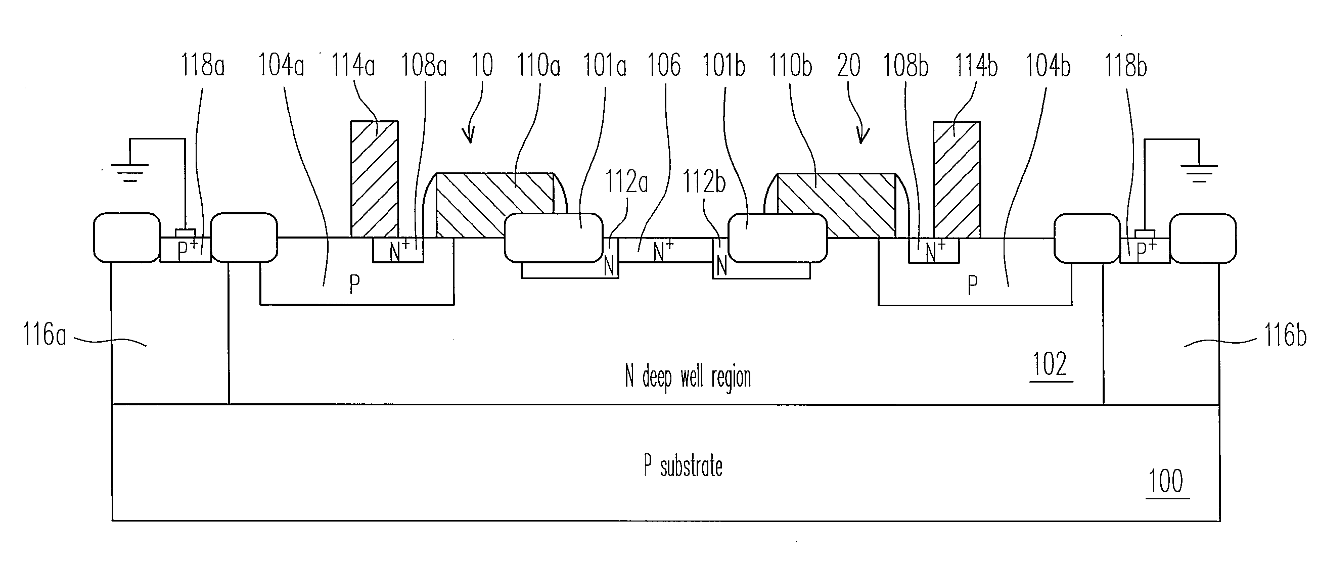
[0030]FIG. 1 schematically illustrates a cross-section view of a LDMOS device for an ESD protection circuit according to an embodiment of the present invention.

[0031]The following embodiment in which the first conductivity type is P-type and the second conductivity type is N-type is provided for illustration purposes, and is not to construed as limiting the scope of the present invention. It is appreciated by persons skilled in the art that the first conductivity type can be N-type and the second conductivity type can be P-type.

[0032]Referring to FIG. 1, the LDMOS devices 10 and 20 for an ESD protection circuit (ESD LDMOS devices 10 and 20) includes a substrate 100 of a first conductivity type, and a deep well region 102 of a second conductivity type. In this embodiment, two ESD LDMOS devices 10 and 20 are provided for illustration purposes and are not to be construed as limiting the scope of the present invention. The number of the ESD LDMOS devices is not limited by the present in...


PUM


Abstract

A LDMOS device for an ESD protection circuit is provided. The LDMOS device includes a substrate of a first conductivity type, a deep well region of a second conductivity type, a body region of the first conductivity type, first and second doped regions of the second conductivity type, and a gate electrode. The deep well region is disposed in the substrate. The body region and the first doped region are respectively disposed in the deep well region. The second doped region is disposed in the body region. The gate electrode is disposed on the deep well region between the first and second doped regions. It is noted that the body region does not include a doped region of the first conductivity type having a different doped concentration from the body region.

Description

BACKGROUND OF THE INVENTION[0001]1. Field of Invention[0002]The present invention relates to a semiconductor device, and more particularly to a lateral double diffused metal oxide semiconductor (LDMOS) device for an electrostatic discharge (ESD) protection circuit.[0003]2. Description of Related Art[0004]ESD is a phenomenon of electrostatic motion along a nonconductive surface. Semiconductor devices and circuits in ICs can be damaged by ESD. For example, a charge carrying object, such as a human body walking on a carpet, a machine for packaging ICs or an apparatus for testing ICs, can discharge to the IC chip when they are in contact with each other. Thus, the IC chip is damaged or broken by the transient power of ESD.[0005]Therefore, a number of methods have been developed to protect semiconductor integrated circuit devices against possible ESD damages. The most common type of ESD protection is the incorporation of a special hardware inside the package. In other words, a specially ...

Claims


Application Information

Patent Timeline
Patent Type & Authority Applications(United States)
IPC IPC(8): H01L29/78
CPCH01L27/0266H01L29/0653H01L29/0878H01L29/7816H01L29/1095H01L29/42368H01L29/47H01L29/1087
Inventor WANG, CHANG-TZUTANG, TIEN-HAO
Owner UNITED MICROELECTRONICS CORP
Why Eureka
Try Eureka