Polishing method and apparatus

Active Publication Date: 2010-02-11
EBARA CORP
View PDF6 Cites 11 Cited by
  • Summary
  • Abstract
  • Description
  • Claims
  • Application Information

AI Technical Summary

Benefits of technology

[0076](1) By performing an inspection on whether or not there is a remaining film such as a metal film (or conductive film) on a substrate such as a semiconductor wafer during polishing, inspection time can be shortened and substrate processing capability can be improved.
[0077](2)

Problems solved by technology

However, in some cases, the semiconductor wafer is cracked or damaged during polishing.
Thus, when the semiconductor wafer is cracked or damaged during polishing of the semiconductor wafer, fragments of the broken semiconductor wafer are scattered on the polishing pad.
In the case where this polishing pad is reused, a surface of a subsequent semiconductor wafer to be polished will be damaged, and thus the polishing pad must be replaced with a new one every t

Method used


Image

  • Polishing method and apparatus
  • Polishing method and apparatus
  • Polishing method and apparatus

Examples


Example

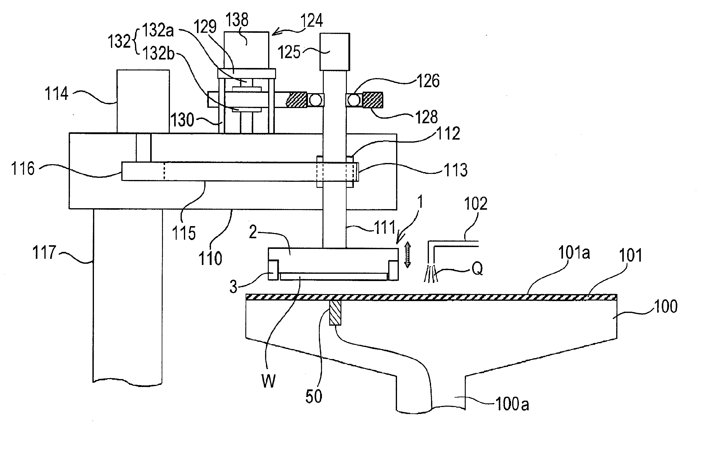
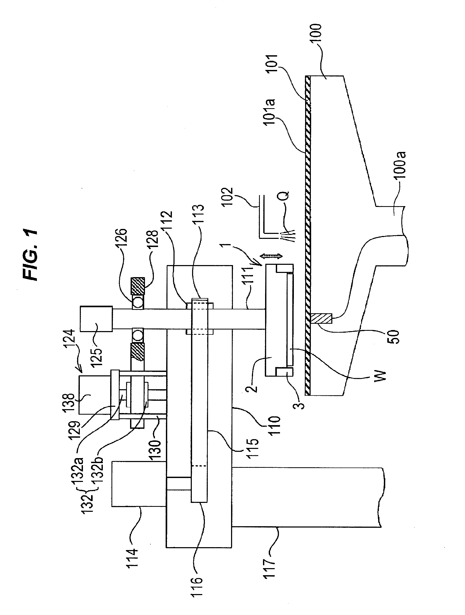
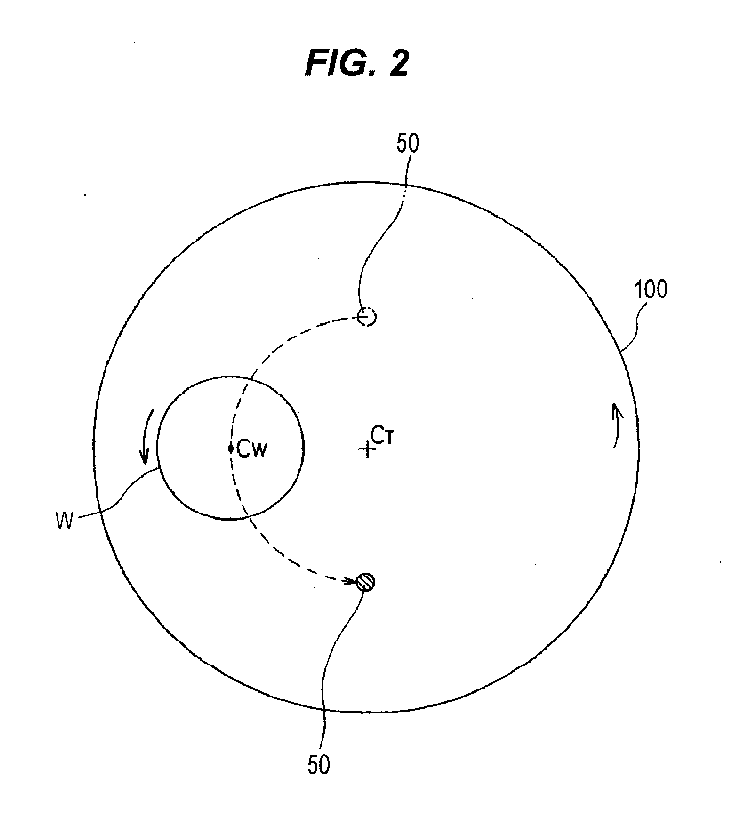
[0118]A polishing apparatus according to embodiments of the present invention will be described below with reference to FIGS. 1 through 27. Like or corresponding structural elements are denoted by like or corresponding reference numerals in FIGS. 1 through 27 and will not be described below repetitively.

[0119]FIG. 1 is a schematic view showing an entire structure of a polishing apparatus according to the present invention. As shown in FIG. 1, the polishing apparatus comprises a polishing table 100, and a top ring 1 for holding a substrate such as a semiconductor wafer as an object to be polished and pressing the substrate against a polishing surface on the polishing table.

[0120]The polishing table 100 is coupled via a table shaft 100a to a motor (not shown) disposed below the polishing table 100. Thus, the polishing table 100 is rotatable about the table shaft 100a. A polishing pad 101 is attached to an upper surface of the polishing table 100. An upper surface 101a of the polishing...


PUM


Abstract

The present invention relates to a polishing method and apparatus for polishing and planarizing an object to be polished (substrate) such as a semiconductor wafer. The substrate as an object to be polished is pressed against a polishing surface on a rotating polishing table in the polishing method. During polishing of the substrate, the polishing table is rotated, and the surface, being polished, of the substrate is scanned by an eddy current sensor provided in the polishing table. An output of the eddy current sensor obtained by scanning the surface, being polished, of the substrate is monitored, and damage of the substrate is detected from a change in the output of the eddy current sensor. Further, an output of an endpoint detecting sensor obtained by scanning the surface, being polished, of the substrate is monitored, and the polishing end point is detected from a change in the output of the end point detecting sensor. After detecting the polishing end point, an output of the endpoint detecting sensor or a different sensor is monitored, and monitoring of the remaining film for detecting a film left on a part of the substrate is performed.

Description

BACKGROUND OF THE INVENTION[0001]1. Field of the Invention[0002]The present invention relates to a polishing method and apparatus, and more particularly to a polishing method and apparatus for polishing and planarizing an object to be polished (substrate) such as a semiconductor wafer.[0003]2. Description of the Related Art[0004]In recent years, high integration and high density in semiconductor device demands smaller and smaller wiring patterns or interconnections and also more and more interconnection layers. Multilayer interconnections in smaller circuits result in greater steps which reflect surface irregularities on lower interconnection layers. An increase in the number of interconnection layers makes film coating performance (step coverage) poor over stepped configurations of thin films. Therefore, better multilayer interconnections need to have the improved step coverage and proper surface planarization. Further, since the depth of focus of a photolithographic optical system...

Claims


Application Information

Patent Timeline
IPC IPC(8): B24B49/00
CPCB24B49/105B24B37/013
Inventor TAKAHASHI, TARONIIJIMA, MOTOHIROOGAWA, AKIHIKO
Owner EBARA CORP
Why Eureka
Try Eureka