Semiconductor device and manufacturing method thereof
Active Publication Date: 2014-02-06
TOYOTA JIDOSHA KK +1
View PDF3 Cites 60 Cited by
Summary
Abstract
Description
Claims
Application Information
AI Technical Summary
This helps you quickly interpret patents by identifying the three key elements:
Problems solved by technology
Method used
Benefits of technology
Benefits of technology
The patent text describes a semiconductor device and a method of manufacturing it that does not require flipping the semiconductor element. This reduces the time needed for inspection.
Problems solved by technology
An IGBT has the high speed and the power durability of a current-drive system bipolar transistor, and the thrifty power consumption of a voltage-drive system bipolar transistor.
Therefore, the inspection takes more time to perform.
Also, the foregoing problems are also common among semiconductor devices in which two IGBTs are arranged in parallel.
Moreover, the foregoing problems are not limited to IGBTs, but are also common among semiconductor devices in which two of any of a variety of types of semiconductor elements including three-terminal elements or two-terminal elements are connected in series or in parallel.
Method used
Image
Click on the blue label to locate the original text in one second.
Reading with bidirectional positioning of images and text.
Examples
first example embodiment
[0052]First, a semiconductor device and a manufacturing method thereof according to a first example embodiment of the invention will be described. The semiconductor device according to this example embodiment has an Insulated-Gate Bipolar Transistor (hereinafter referred to as “IGBT”) as a semiconductor element.
[0053]First, the semiconductor device according to this example embodiment will be described.
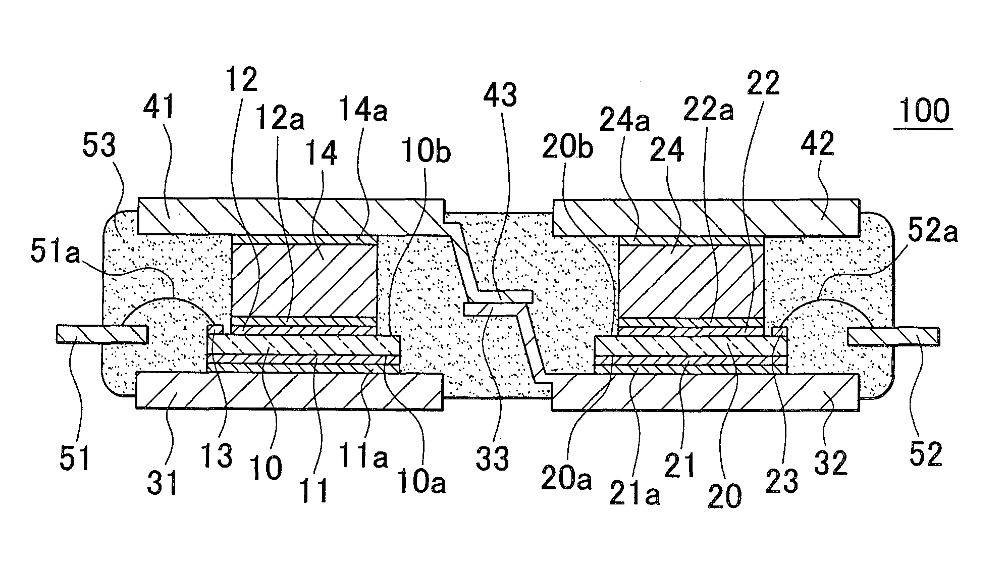
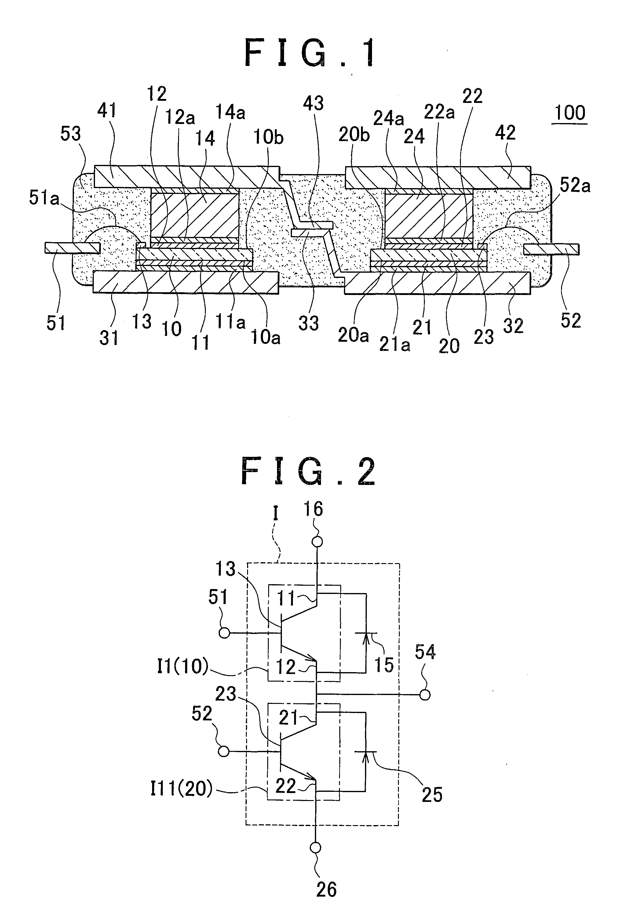
[0054]FIG. 1 is a sectional view showing a frame format of the structure of the semiconductor device according to this example embodiment.
[0055]The semiconductor device 100 includes a first semiconductor element 10, a second semiconductor element 20, a first thick plate portion 31, a second thick plate portion 32, a first thin plate portion 33, a third thick plate portion 41, a fourth thick plate portion 42, a second thin plate portion 43, a first control electrode terminal 51, a second control electrode terminal 52, and an encapsulation resin portion 53.
[0056]The first semiconductor ...
second example embodiment
[0149]Next, a semiconductor device and a manufacturing method thereof according to a second example embodiment of the invention will be described.
[0150]The semiconductor device according to this example embodiment differs from the semiconductor device according to the first example embodiment in that two semiconductor elements are connected in parallel.
[0151]First, the semiconductor device according to this example embodiment will be described.
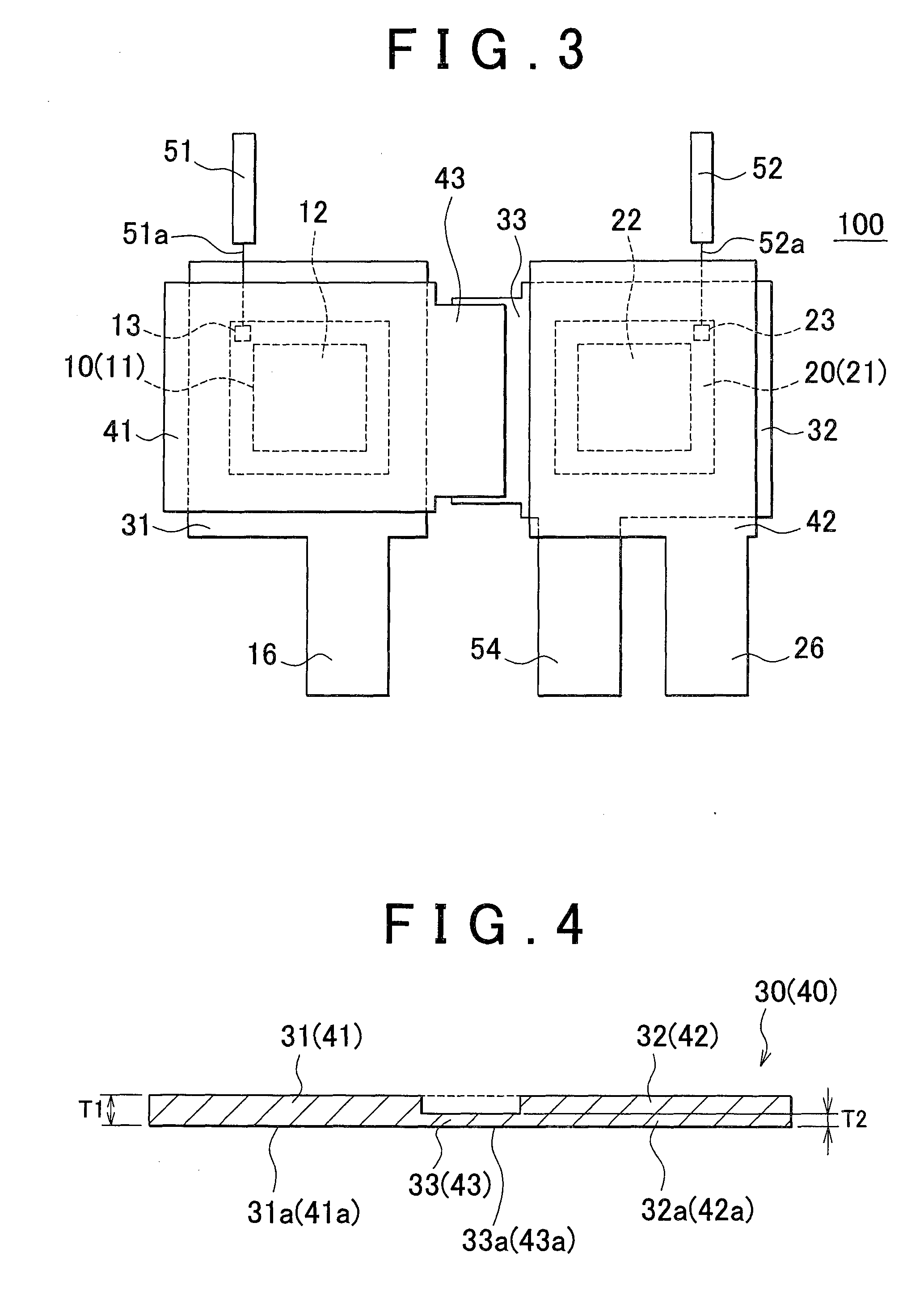
[0152]FIG. 10 is a sectional view showing a frame format of the structure of the semiconductor device according to this example embodiment.
[0153]A semiconductor device 100b includes a first semiconductor element 10, a second semiconductor element 20, a first thick plate portion 31, a second thick plate portion 32, a first thin plate portion 33, a third thick plate portion 41, a fourth thick plate portion 42, a second thin plate portion 43, a first control electrode terminal 51, a second control electrode terminal 52, and an encapsulation resin...
third example embodiment
[0174]FIG. 13 is an external perspective view of an example of a semiconductor device 100c according to a third example embodiment of the invention. In this third example embodiment, constituent elements that are the same as constituent elements in the example embodiments described thus far will be denoted by like reference characters, and descriptions of those constituent elements will be omitted.
[0175]In FIG. 13, the semiconductor device 100c according to the third example embodiment includes a third thick plate portion 41, a fourth thick plate portion 42, encapsulation resin 55, a high-order side power supply connecting terminal 16, a low-order side power supply connecting terminal 26, an output terminal 54, a first control electrode terminal 51, and a second control electrode terminal 52. In FIG. 13, the center portion formed by the third thick plate portion 41, the fourth thick plate portion 42, and the encapsulation resin 55 is a semiconductor element carrying portion that inc...
PUM
Abstract
A semiconductor device includes a first semiconductor element; a first thick plate portion that is electrically connected to an electrode on a lower surface side of the first semiconductor element, and is formed by a conductor; a second semiconductor element that is arranged such that a main surface of the second semiconductor element faces a main surface of the first semiconductor element; a second thick plate portion that is electrically connected to an electrode on a lower surface side of the second semiconductor element, and is formed by a conductor; a third thick plate portion that is electrically connected to an electrode on an upper surface side of the first semiconductor element, and is formed by a conductor; a fourth thick plate portion that is electrically connected to an electrode on an upper surface side of the second semiconductor element, and is formed by a conductor; a first thin plate portion that is provided on the second thick plate portion, is formed by a conductor, and is thinner than the second thick plate portion; and a second thin plate portion that is provided on the third thick plate portion, is formed by a conductor, and is thinner than the third thick plate portion. The first thin plate portion and the second thin plate portion are fixed together and electrically connected.
Description
BACKGROUND OF THE INVENTION[0001]1. Field of the Invention[0002]The invention relates to a semiconductor device and a manufacturing method thereof.[0003]2. Description of Related Art[0004]The demand for a power semiconductor device having a power semiconductor element, and a power semiconductor module provided with a power semiconductor device, is increasing due to an increase in demand for power equipment having a function of a power control circuit power or a power converter circuit such as an inverter or a converter.[0005]Insulated Gate Bipolar Transistors (IGBTs) are used as power semiconductor elements. An IGBT is a semiconductor element in which a base of a bipolar transistor has been replaced with a gate of a field-effect transistor (referred to as a “FET”). An IGBT has the high speed and the power durability of a current-drive system bipolar transistor, and the thrifty power consumption of a voltage-drive system bipolar transistor.[0006]Japanese Patent Application Publicatio...
Claims
Application Information
Patent Timeline
Application Date:The date an application was filed.
Publication Date:The date a patent or application was officially published.
First Publication Date:The earliest publication date of a patent with the same application number.
Issue Date:Publication date of the patent grant document.
PCT Entry Date:The Entry date of PCT National Phase.
Estimated Expiry Date:The statutory expiry date of a patent right according to the Patent Law, and it is the longest term of protection that the patent right can achieve without the termination of the patent right due to other reasons(Term extension factor has been taken into account ).
Invalid Date:Actual expiry date is based on effective date or publication date of legal transaction data of invalid patent.

