Light emitting device and production method of same

a technology of light emitting diodes and production methods, which is applied in the direction of semiconductor/solid-state device manufacturing, semiconductor devices, electrical devices, etc., can solve the problems of failure of the light emitting diodes themselves, and sub-mounted types also had problems, so as to achieve high strength, withstand large current and thermal stress, and improve the effect of productivity

Inactive Publication Date: 2010-02-18
CI KASEI COMPANY
View PDF5 Cites 43 Cited by
  • Summary
  • Abstract
  • Description
  • Claims
  • Application Information

AI Technical Summary

Benefits of technology

[0018]In order to solve the aforementioned problems, an object of the present invention is to provide a light emitting device having for a light source thereof a vertical geometry light emitting diode that has superior productivity, is

Problems solved by technology

In contrast to vertical geometry light emitting diodes allowing a larger current flow and improved luminosity, since configurations of the submounted type have difficulty in dissipating heat generated from the light emitting diode due to poor thermal conductivity, the package easily reaches a high temperature thereby resulting in the disadvantages of wiring disconnections occurring during the course of use or failure of the light emitting diode itself.
In addition, submounted types also had the problem of poor productivity.
Consequently, in the case of connections by bonding using gold wires, vibrations and pressure generated impart a stimulus to the semiconductor layer and light emitting layer of the upper portion of the vertical geometry light emitting diode through the upper electrode, possibly resulting in damage thereto.
Consequently, it is necessary to subtly adjust the pressure and ultrasonic oscillation of the wire bonder to prevent damage to the semiconductor layer and light emitting layer of a vertical geometry light emitting diode caused by vibrations and pressure, resulting in a tendency for an increase in the connection resistance of the gold wires.
In this case, since there are limitati

Method used


Image

  • Light emitting device and production method of same
  • Light emitting device and production method of same
  • Light emitting device and production method of same

Examples


Embodiment Construction

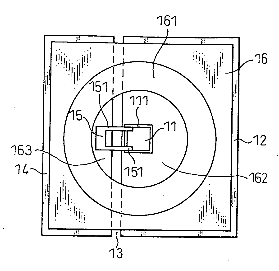
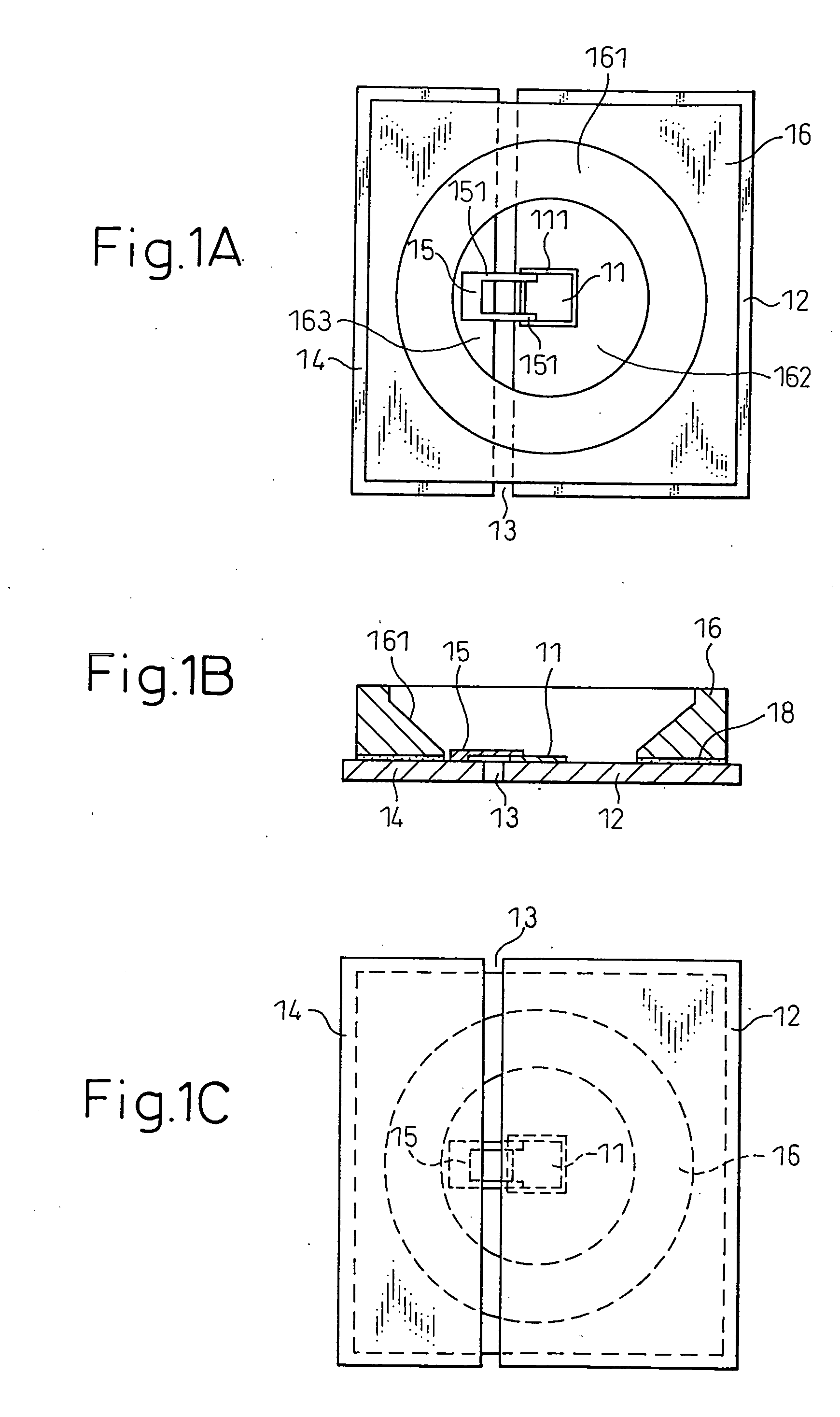
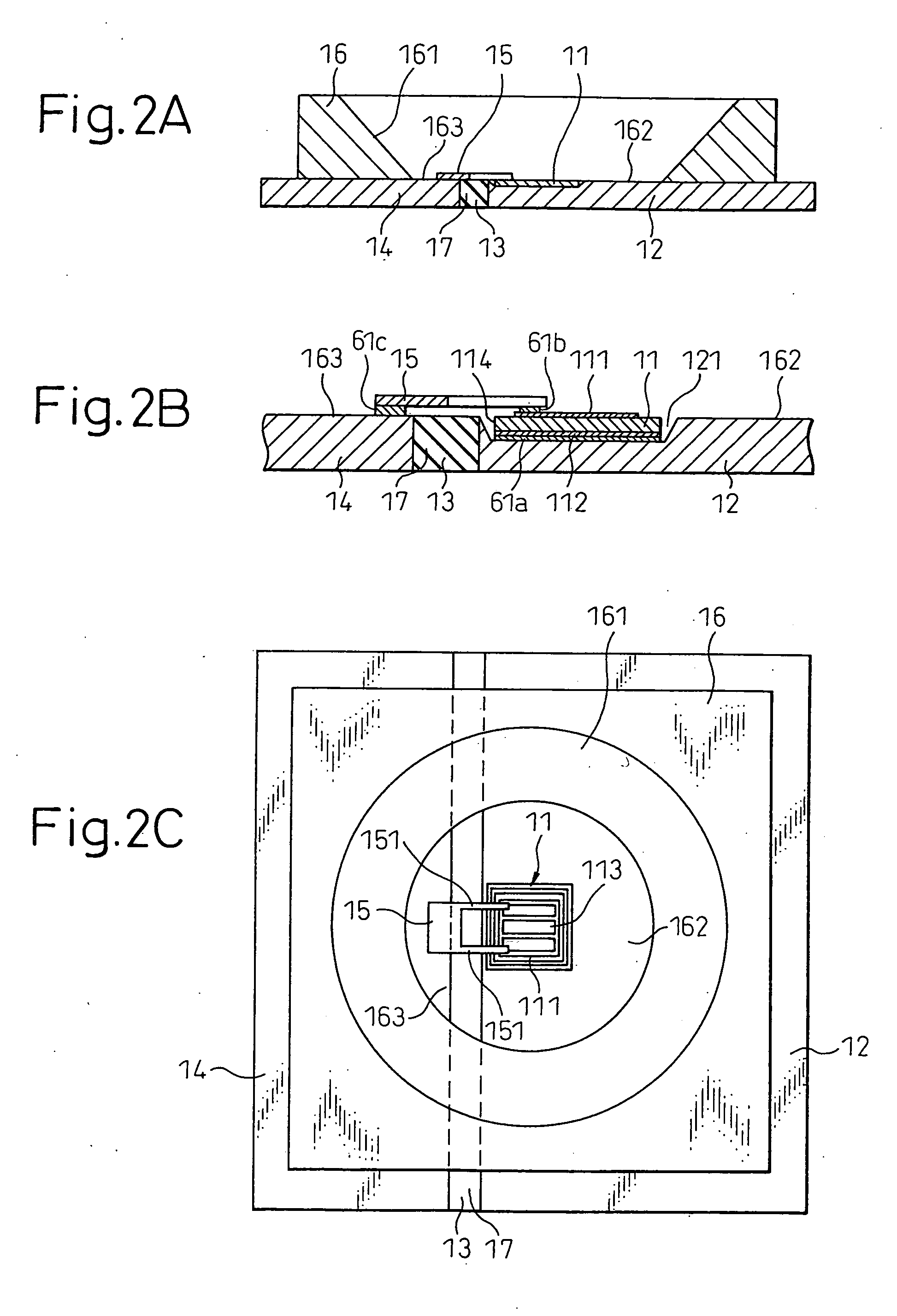
[0055]In a light emitting device of the present invention having for a light source thereof a vertical geometry light emitting diode, the vertical geometry light emitting diode is mounted on a package by joining a lower electrode thereof to one of the package electrodes, while an upper electrode of the light emitting diode is connected to another package electrode by an electrically conductive connecting member.

[0056]In the case where a substrate that comprises the package is made of metal, each of two mutually separated substrate portions that comprise the substrate can be used as two mutually separated package electrodes.

[0057]The package substrate in the light emitting device of the present invention may also be made of ceramic. In this case, the package electrodes are formed mutually separated using a conductor material on the ceramic substrate.

[0058]A package having three or more package electrodes can also be used.

[0059]The following provides an explanation of a light emitting...


PUM


Abstract

A light emitting device, and a production method thereof, is provided having for a light source thereof a vertical geometry light emitting diode, that allows a large current to flow through the vertical geometry light emitting diode and takes into consideration the dissipation of heat occurring at that time or the expansion and contraction of a metal member due to thermal stress caused by that heat. The light emitting device at least comprises a package having a plurality of mutually separated package electrodes; a vertical geometry light emitting diode having a light emitting layer positioned between a p-type semiconductor layer and an n-type semiconductor layer, an upper partial electrode of the uppermost layer, and a lower electrode of the lowermost layer, wherein the lower electrode is joined onto one of the package electrodes; and, a conductive connecting member that connects the upper electrode of the vertical geometry light emitting diode with another of package electrodes; wherein the junction between said one of the package electrodes and the lower electrode, the junction between the upper electrode and the conductive connecting member, and the junction between the conductive connecting member and said other of package electrodes are made with solder.

Description

TECHNICAL FIELD[0001]The present invention relates to a light emitting device having for a light source thereof a vertical geometry light emitting diode provided with an upper electrode and a lower electrode, and to a production method thereof. More particularly, the present invention relates to a light emitting device that allows a large current to flow through a vertical geometry light emitting diode and takes into consideration the dissipation of heat occurring at that time or the expansion and contraction of a metal member due to thermal stress caused by that heat, and to a production method thereof. In addition, the present invention relates to a light emitting device capable of preventing damage to a light emitting layer caused by vibrations or heat by using electrically conductive connecting members joined by soldering instead of connecting gold wires for supplying electrical power to a light emitting diode by wire bonding, and to a production method thereof.BACKGROUND ART[00...

Claims


Application Information

Patent Timeline
IPC IPC(8): H01L33/00H01L33/62
CPCH01L25/0753H01L33/62H01L2224/45144H01L2224/32225H01L2924/01322H01L2924/09701H01L2224/73265H01L2224/48227H01L2224/48091H01L2924/00014H01L2924/00H01L2224/45014H01L2224/85385H01L2924/206
Inventor FUSHIMI, HIROSHINISHIYAMA, KENGOKUDOU, KOUJIYAMAMOTO, ITSUKIMITSUYAMA, KAZUMA
Owner CI KASEI COMPANY
Why Eureka
Try Eureka