

Electronic element wafer module and method for manufacturing electronic element wafer module, electronic element module and method for manufacturing electronic element module, and electronic information device
- Summary
- Abstract
- Description
- Claims
- Application Information
AI Technical Summary
Benefits of technology
Problems solved by technology
Method used
Image

Examples
embodiment 1
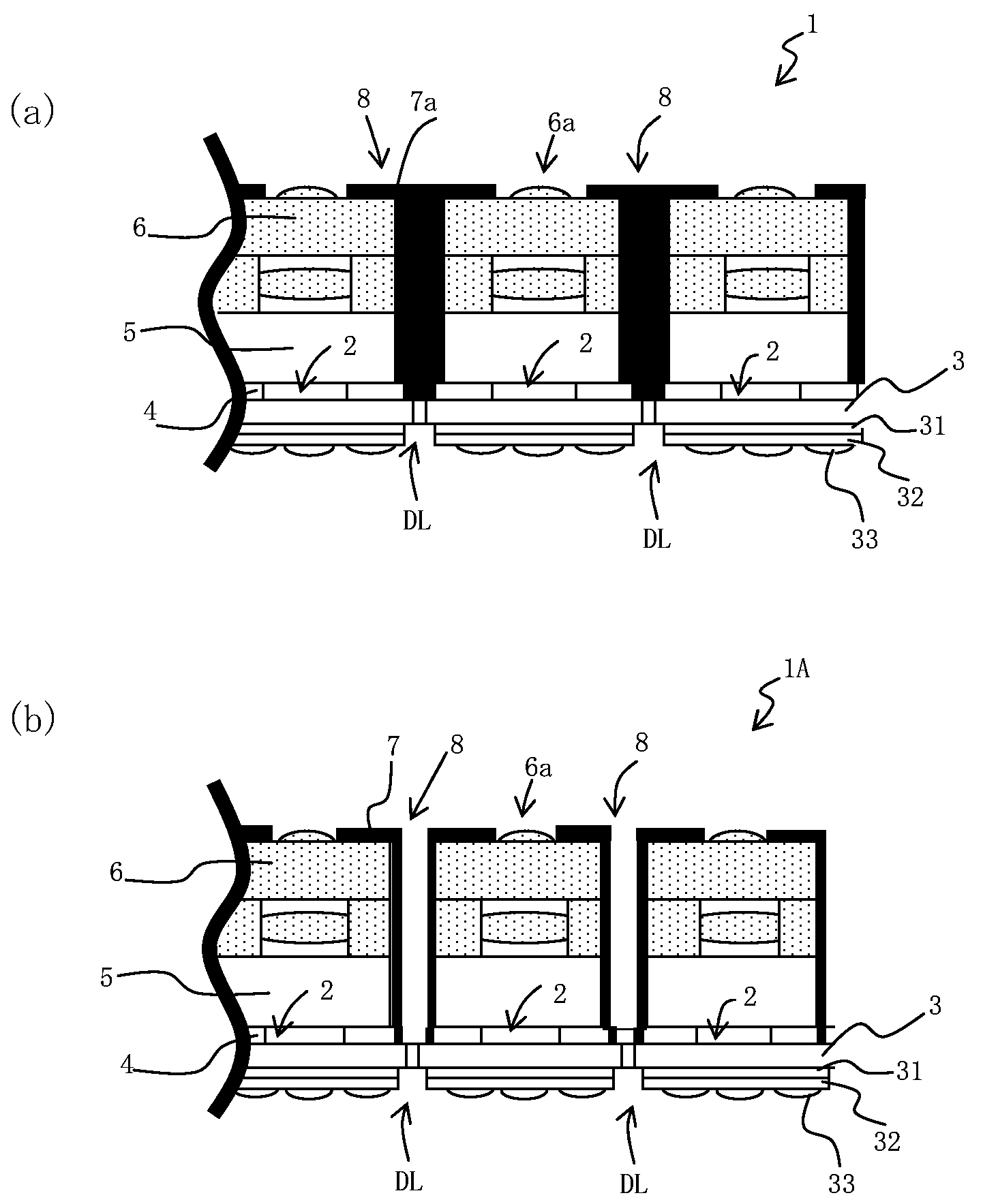
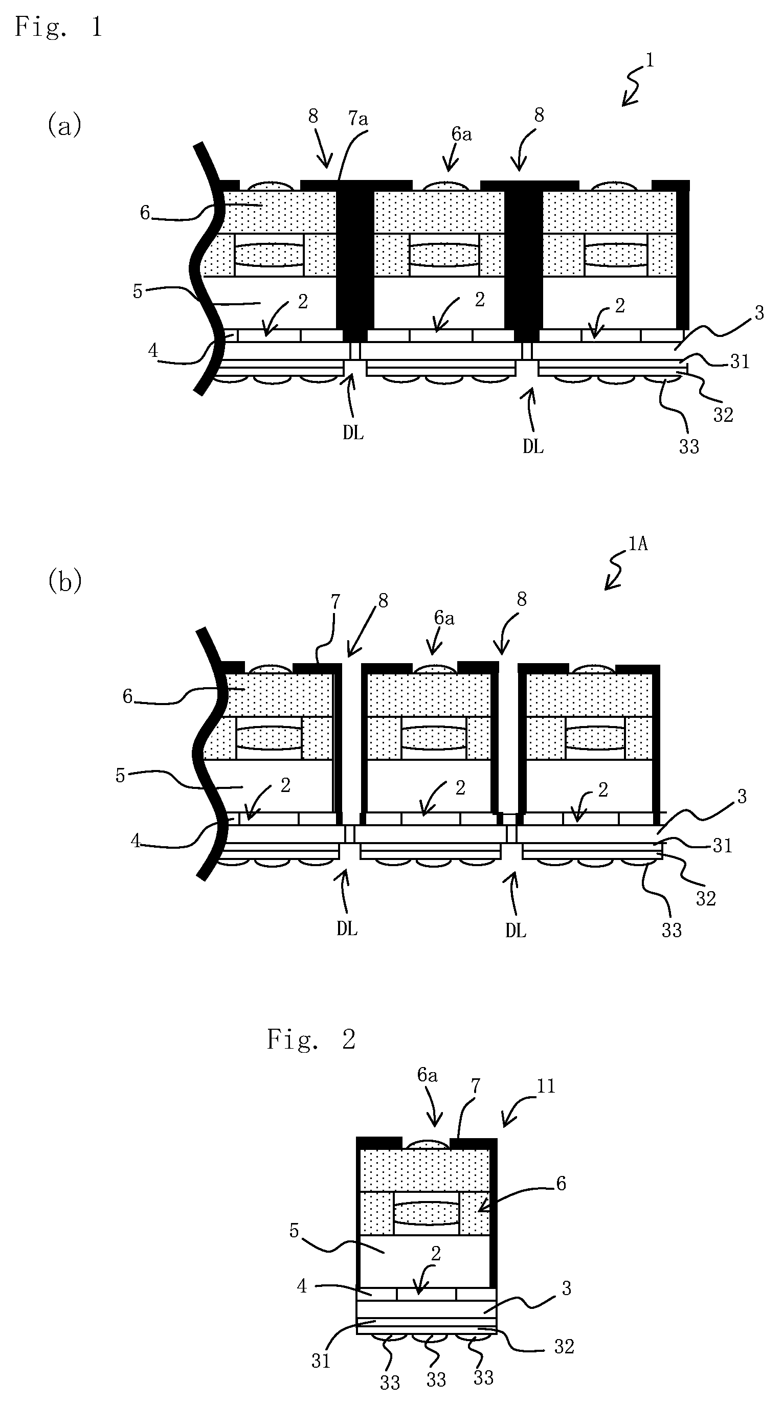
[0081]FIG. 1 is an essential part longitudinal cross sectional view illustrating an exemplary structure of a sensor wafer module according to Embodiment 1 of the present invention. FIG. 1(a) is an essential part longitudinal cross sectional view of the case where a light shielding material is filled in a dicing groove. FIG. 1(b) is an essential part longitudinal cross sectional view of the case where a light shielding material is applied on side surfaces and a bottom surface in a dicing groove.
[0082]In FIGS. 1(a) and 1(b), a sensor wafer module 1, as an electronic element wafer module according to Embodiment 1, includes: a penetrated wafer 3 as an electronic element wafer; a resin adhesion layer 4; a glass plate 5 as a transparent support substrate; a wafer-shaped optical part 6; and a light shielding member 7a (light shielding material). In the sensor wafer module 1, the glass plate 5 and the wafer-shaped optical part 6 are adhered on top of another in this order, being aligned wit...
embodiment 2
[0107]FIG. 6 is a block diagram illustrating an exemplary schematic structure of an electronic information device including a solid-state image capturing apparatus including a sensor module according to Embodiment 1 of the present invention used in an image capturing section thereof, as Embodiment 2 of the present invention.
[0108]In FIG. 6, an electronic information device 90 according to Embodiment 2 of the present invention includes: a solid-state image capturing apparatus 91 for performing various signal processing on an image capturing signal from the sensor module 11 according to Embodiment 1 so as to obtain a color image signal; a memory section 92 (e.g., recording media) for data-recording a color image signal from the solid-state image capturing apparatus 91 after a predetermined signal process is performed on the color image signal for recording; a display section 93 (e.g., a liquid crystal display apparatus) for displaying the color image signal from the solid-state image ...
PUM
 Abstract
Description
Claims
Application Information