Data input/output circuit

Inactive Publication Date: 2010-03-04
SK HYNIX INC
View PDF5 Cites 2 Cited by
  • Summary
  • Abstract
  • Description
  • Claims
  • Application Information

AI Technical Summary

Benefits of technology

[0033]Embodiments of the present invention are directed to providing a data input/ou

Problems solved by technology

If it fails to accurately control the duty cycle ratio, data may be distorted due to lack of data margin.
Therefore, in the conventional data output circuit, a data margin is reduced when the internal data DATA is latched in response to the rising edge o

Method used


Image

  • Data input/output circuit
  • Data input/output circuit
  • Data input/output circuit

Examples


Embodiment Construction

[0046]Other objects and advantages of the present invention can be understood by the following description, and become apparent with reference to the embodiments of the present invention.

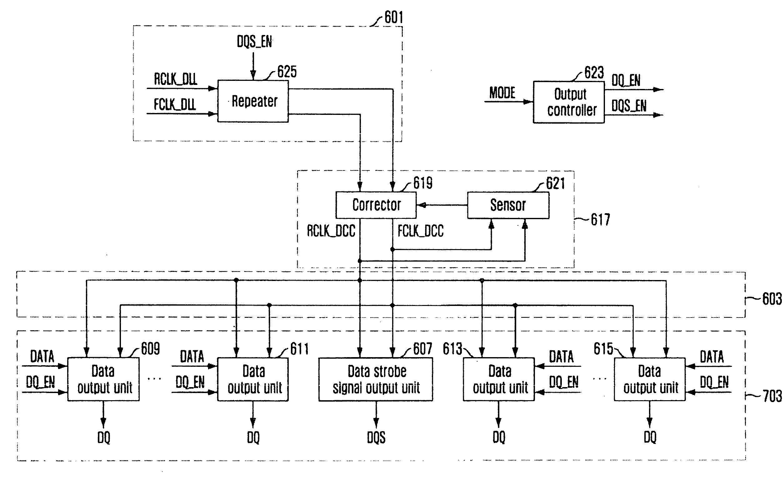
[0047]FIG. 6 is a diagram illustrating a data output circuit in accordance with an embodiment of the present invention.

[0048]Referring to FIG. 6, the data output circuit according to the present embodiment includes an output unit 605, a first transmission line unit 603, a second transmission line unit 601, an output controller 623, and a duty cycle ratio corrector 617.

[0049]Unlike the related art, the data output circuit according to the present embodiment includes a duty cycle ratio corrector 617 disposed between the first transmission line unit 603 and the second transmission line unit 601. Therefore, the data output circuit according to the present embodiment can correct the duty cycle ratio distortion of the internal clocks RCLK_DLL and FCLK_DLL, which may be generated after the internal clocks ...


PUM


Abstract

A data input/output circuit includes an output unit for outputting a first data strobe signal and first data in response to an internal clock generated in a delay locked loop, a first transmission line unit having a clock tree structure for transmitting the internal clock to the output unit, a second transmission line unit for transmitting the internal clock from the delay locked loop to the first transmission line unit, a duty cycle ratio correcting unit interconnected between the first transmission line unit and the second transmission line unit for correcting a duty cycle ratio of the internal clock, a data strobe signal input unit for receiving a second data strobe signal from an outside of a semiconductor memory device and generating an internal data strobe signal, and a plurality of data input units for outputting a second data in response to the internal data strobe signal.

Description

CROSS-REFERENCE TO RELATED APPLICATION[0001]The present invention claims priority of Korean patent application number 10-2008-0086110, filed on Sep. 2, 2008, which is incorporated by reference in its entirety.BACKGROUND OF THE INVENTION[0002]The present invention relates to a data input / output circuit of a semiconductor memory device, and more particularly, to a data input / output circuit having improved jitter characteristics.[0003]A synchronous semiconductor memory device is synchronized with a clock provided from an external device. Particularly, a double data rate (DDR) synchronous semiconductor memory device is synchronized with a rising edge and a falling edge of a clock inputted from an external device, thereby processing two-bit data in one clock cycle. The DDR synchronous semiconductor memory device includes a delay locked loop (DLL) circuit for accurate timing of data input / output.[0004]It is very important to precisely control a duty cycle ratio of a clock in a synchronous...

Claims


Application Information

Patent Timeline
IPC IPC(8): G11C7/00G11C8/18
CPCG11C7/1051G11C7/1066G11C7/222G11C7/1093G11C7/22G11C7/1078
Inventor CHOI, HOONCHUNG, JIN-II
Owner SK HYNIX INC
Why Eureka
Try Eureka