Method and electronic computing circuit for operand width reduction for a modulo adder followed by saturation concurrent message processing

a technology of modulo adder and electronic computing circuit, which is applied in the field of computer chip design, can solve the problems of increasing the delay of these functions, reducing the design time, and specific instructions sometimes making a more complex design necessary

Inactive Publication Date: 2010-03-04
IBM CORP
View PDF1 Cites 0 Cited by
  • Summary
  • Abstract
  • Description
  • Claims
  • Application Information

AI Technical Summary

Benefits of technology

[0033]providing an output comprising said two M-bit output operands allowing

Problems solved by technology

In modern chip design the reduction of design time is a critical issue.
However, for different operations executed by a similar unit, specific instructions sometimes make a more complex design necessary.
A disadvantage of this micro architecture is that the adder device must be adapted to process inp

Method used


Image

  • Method and electronic computing circuit for operand width reduction for a modulo adder followed by saturation concurrent message processing
  • Method and electronic computing circuit for operand width reduction for a modulo adder followed by saturation concurrent message processing
  • Method and electronic computing circuit for operand width reduction for a modulo adder followed by saturation concurrent message processing

Examples


first embodiment

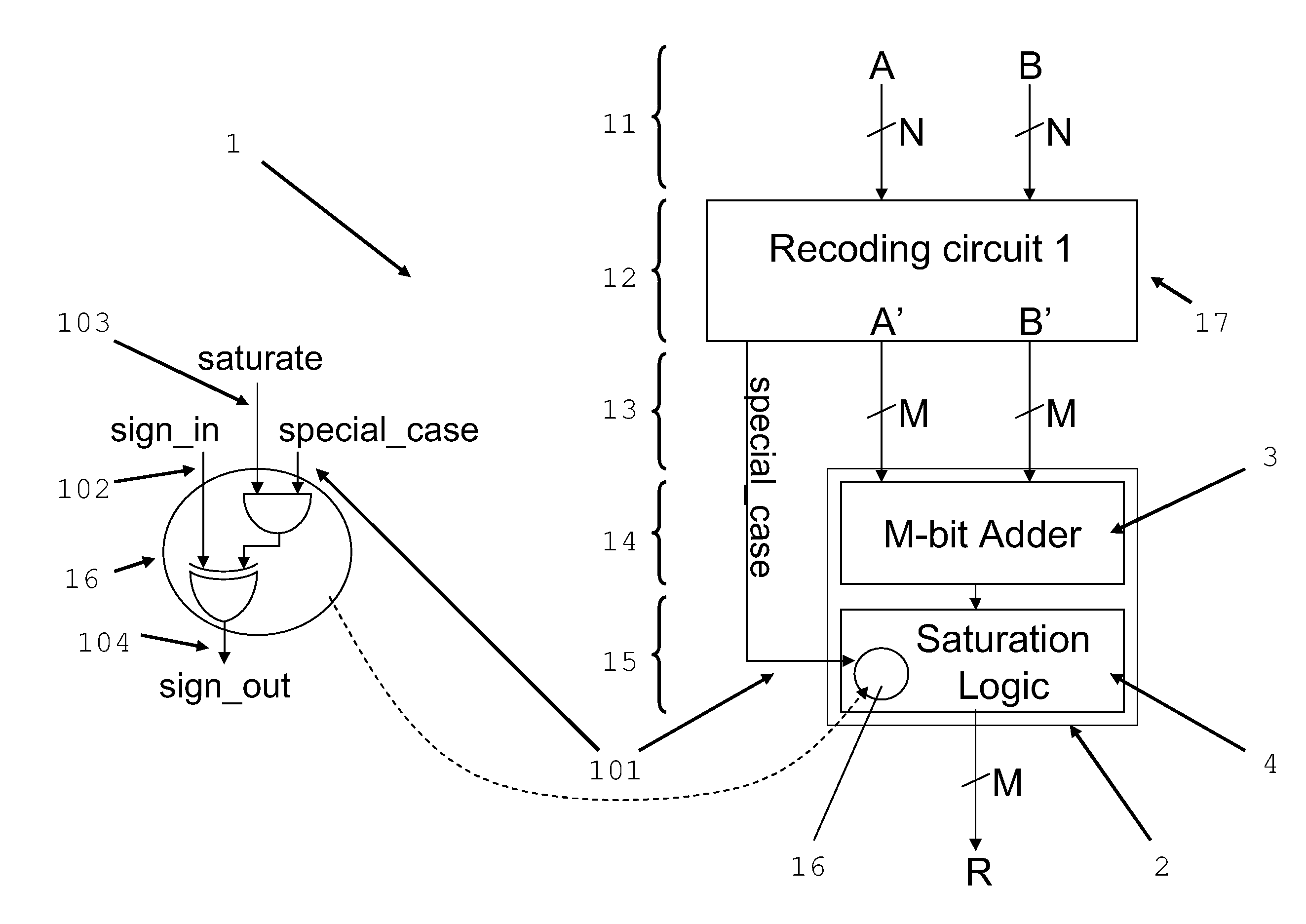
[0047]FIG. 1. shows a schematic block diagram representation of an electronic computing circuit 1 to be used to perform a first method according to the invention.

[0048]The electronic computing circuit 1 comprises a recoding circuit 17 and a circuit 16 arranged within a saturation circuit 4 of a saturation adder 2. The recoding circuit 17 processes two N-bit input operands A, B of a bit width of N and generates two M-bit output operands A′, B′ of a reduced bit width of M in a way, that a post-processing performed on said two M-bit output operands A′, B′ by the saturation adder 2 provides an M-bit result equal to the M-bit result of an N-bit modulo addition of the two N-bit input operands A, B followed by an saturation to M bits. The saturation adder 2 comprises an M-bit adder 3 and the saturation logic 4 in order to perform an M-bit adder function followed by saturation to M bits.

[0049]In a first step 11 two N-bit input operands A, B with a bit width N are received as input.

[0050]In ...

second embodiment

[0060]FIG. 4. shows a schematic block diagram representation of an electronic computing circuit 5 to be used to perform a second method according to the invention. The electronic computing circuit 5 comprises a recoding circuit 47 and an overflow sign calculation circuit 48. Also the recoding circuit 47 processes two N-bit input operands A, B of a bit width of N and generates two M-bit output operands A′, B′ of a reduced bit width of M in a way, that a post-processing performed on said two M-bit output operands A′, B′ by a saturation adder 6 provides an M-bit result equal to the M-bit result of an N-bit modulo addition of the two N-bit input operands A, B followed by an saturation to M bits. The saturation adder 6 comprises an M-bit adder 7 and the saturation logic 8 in order to perform an M-bit adder function followed by saturation to M bits.

[0061]In a first step 41 the external overflow sign calculation circuit 48 computes an overflow sign signal 49 that indicates the sign of the ...


PUM


Abstract

A method for operand width reduction is described, wherein two N-bit input operands (A, B) of a bit width of N are processed and two M-bit output operands (A′, B′) of a reduced bit width of M are generated in a way, that a post-processing comprising an M-bit adder function followed by saturation to M bits performed on said two M-bit output operands (A′, B′) provides an M-bit result equal to an M-bit result of an N-bit modulo adder function of the two N-bit input operands (A, B), followed by a saturation to M bits. Further an electronic computing circuit (1, 5) is described performing said method. Additionally a computer system comprising such an electronic computing circuit is described.

Description

BACKGROUND OF THE INVENTION[0001]The invention lies within the field of computer chip design. More particularly, the invention relates to a method and an electronic computing circuit for operand width reduction for modulo adder followed by saturation.[0002]In modern chip design the reduction of design time is a critical issue. Reuse of building blocks enables a reduction of design effort and design time. However, for different operations executed by a similar unit, specific instructions sometimes make a more complex design necessary. This especially applies for Single-Instruction-Multiple-Data (SIMD) units like e.g. Vector Multimedia Extension (VMX), Synergistic Processing Elements (SPE) or Supplemental Streaming SIMD Extensions 4 (SSE4) units. The data width, i.e. bit width, in these units is variable and depends on the instruction to be performed. The common bit widths are by the power of two, like 8, 16, 32, 64, etc. Operands and results are always of these bit widths.[0003]In ma...

Claims


Application Information

Patent Timeline
IPC IPC(8): G06F7/50
CPCG06F7/727G06F7/499
Inventor GEMMEKE, TOBIASMAEDING, NICOLASPREISS, JOCHEN
Owner IBM CORP
Why Eureka
Try Eureka