Systems and Methods Utilizing Redundancy in Semiconductor Chip Interconnects

a technology of redundancy and interconnects, applied in logic circuits, instruments, and increasing modifications to ensure reliability, can solve problems such as failure and yield, and should be presented to every device that experiences an interconnect failure, and low yield is generally considered to be unacceptabl

Active Publication Date: 2010-03-11
QUALCOMM INC
View PDF5 Cites 140 Cited by
  • Summary
  • Abstract
  • Description
  • Claims
  • Application Information

AI Technical Summary

Benefits of technology

[0006]Various embodiments of the present disclosure include an integrated circuit (IC) that comprise a primary interconnect and a redundant interconnec

Problems solved by technology

As die stacks use more and more interconnects, issues of failure and yield are presented.
For instance, if a failure rate for a particular high-density interconnect is one in one thousand, and there are one thousand of the high-density interconnects in each device, then

Method used


Image

  • Systems and Methods Utilizing Redundancy in Semiconductor Chip Interconnects
  • Systems and Methods Utilizing Redundancy in Semiconductor Chip Interconnects
  • Systems and Methods Utilizing Redundancy in Semiconductor Chip Interconnects

Examples


Embodiment Construction

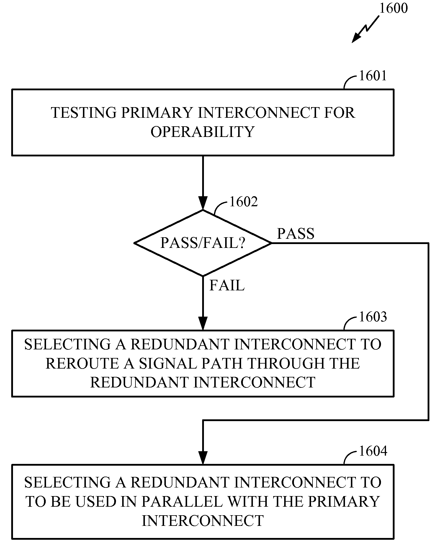
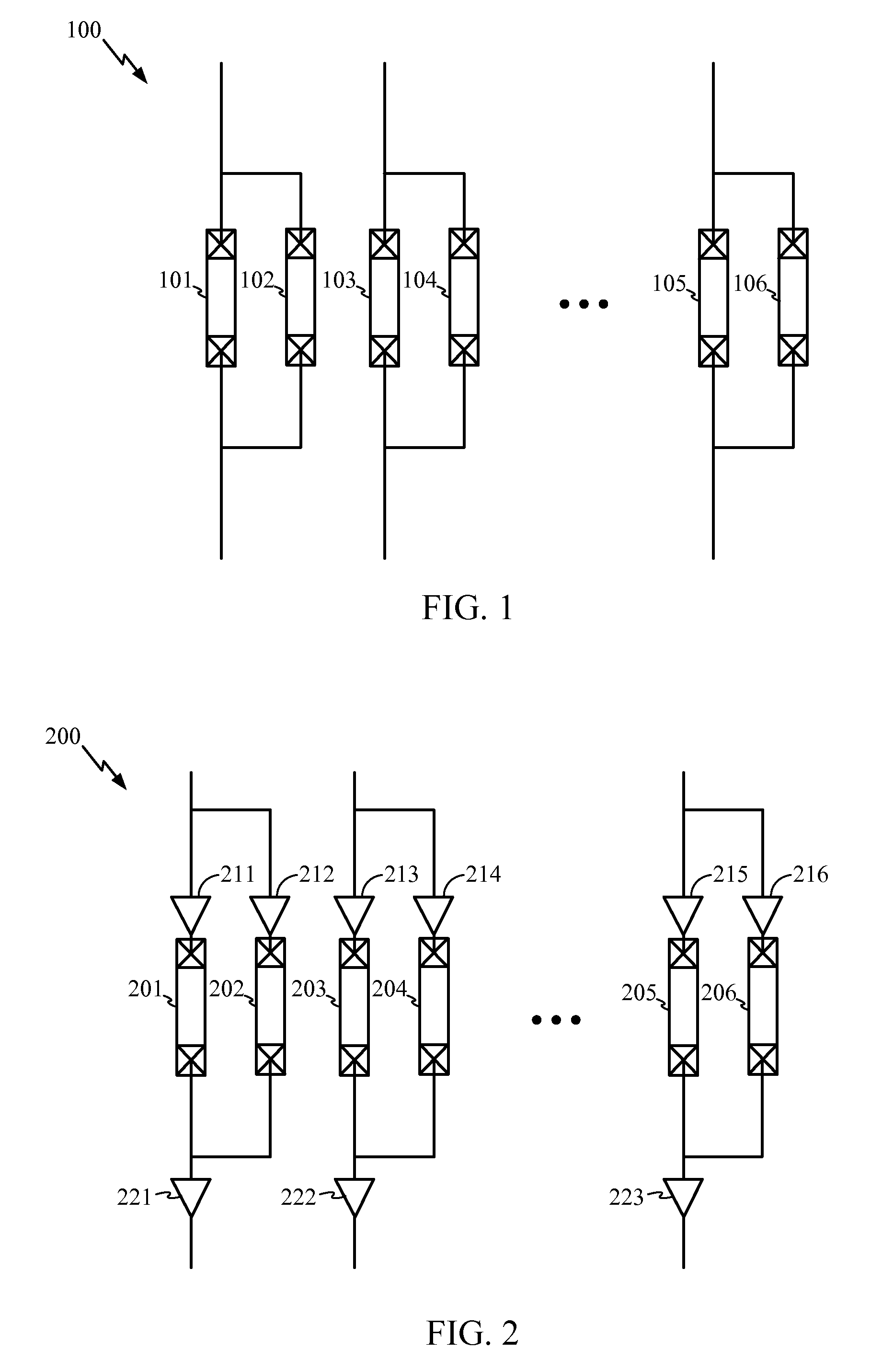
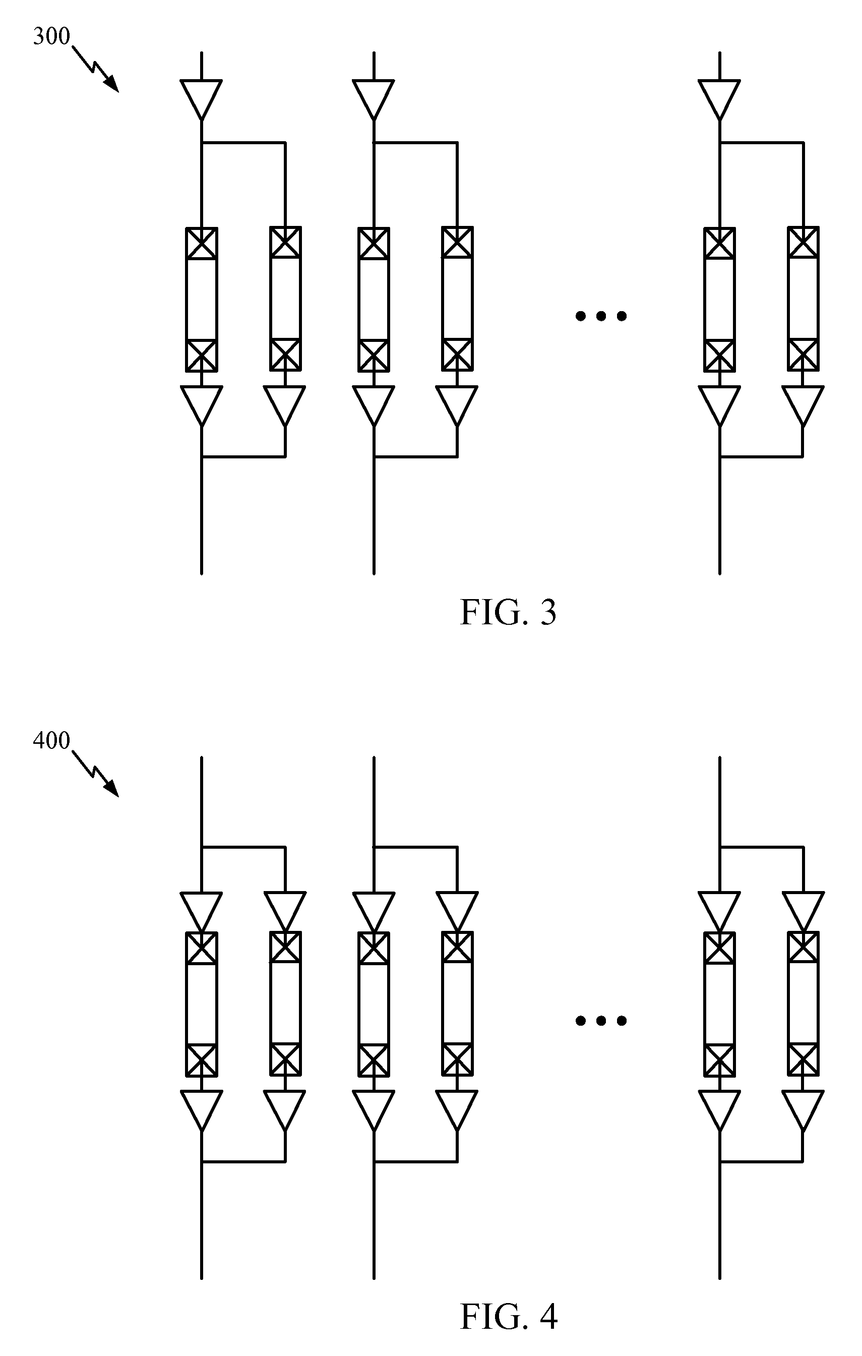
[0030]Various embodiments of the present disclosure include systems and methods that employ redundancy in interconnects and can be used to compensate for interconnect failure as well as to increase bandwidth. For example, some embodiments employ Through Silicon Vias (TSVs), which are one kind of interconnect. TSVs include conductive vias that extend through the semiconductor material of chips. TSVs can be used in a die stack to provide communication between components in different layers and 3D TSVs can be used in a monolithic manufacturing process to provide communication between stacked layers in the same manufacturing process. One example embodiment uses TSVs for die-to-die communications and, more specifically, uses one or more redundant TSVs to correct defects and / or to improve performance. In this example, when it is discovered post-fabrication that one of the TSVs is defective, signals that would ordinarily be conveyed with that particular TSV can be rerouted through an adjac...


PUM


Abstract

An integrated circuit, or combination of integrated circuits, has a primary interconnect, a redundant interconnect, and circuitry connecting the primary and redundant interconnects allowing selection of the redundant interconnect to bypass the primary interconnect.

Description

CROSS REFERENCE TO RELATED APPLICATION[0001]This application claims the benefit of U.S. Provisional Patent Application No. 61 / 095,855 filed Sep. 10, 2008.TECHNICAL FIELD[0002]The present disclosure generally relates to semiconductor chips and, more specifically, to redundant interconnects in semiconductor chips.BACKGROUND[0003]Current technology employs stacking semiconductor chips (e.g., microprocessors, digital signal processors, etc.) or arranging the chips side-by-side. Communication between the chips is sometimes achieved by connecting them using bond wires that hang loose outside of the die space of the chips. Other embodiments use Through Silicon Vias (TSVs) instead of, or in addition to, bond wires. Bond wires, TSVs, and the like are generally referred to as “interconnects.”[0004]As die stacks use more and more interconnects, issues of failure and yield are presented. For instance, if a failure rate for a particular high-density interconnect is one in one thousand, and there...

Claims


Application Information

Patent Timeline
IPC IPC(8): H03K19/003
CPCH01L25/0657H01L2225/06513H01L2225/06527H01L2225/06541H01L2924/0002H01L2225/06596H01L2924/00H01L22/22G11C29/816
Inventor LAISNE, MICHAELARABI, KARIMPETROV, TSVETOMIR
Owner QUALCOMM INC
Why Eureka
Try Eureka