Solid-state imaging apparatus, imaging system and driving method for solid-state imaging apparatus

a technology of imaging apparatus and solid-state imaging, which is applied in the direction of color television details, television system details, television systems, etc., can solve the problems of inability to examine addition or averaging, resolution falls, and loss of signals, so as to reduce jaggy and increase the speed of operation

Active Publication Date: 2010-03-11
CANON KK
View PDF23 Cites 24 Cited by
  • Summary
  • Abstract
  • Description
  • Claims
  • Application Information

AI Technical Summary

Benefits of technology

[0008]It is an object of the present invention to provide a solid-state imaging apparatus, an imaging system and a driving method for the solid-state imaging apparatus that can reduce jaggy while increasing speed of operation for reading out signals.

Problems solved by technology

When an increase in speed is realized by the thinning-out, signals are lost and resolution falls.
However, in Japanese Patent Application Laid-Open No. 2001-45378, considering that resolution falls when signals are added, the addition or averaging is not examined.

Method used


Image

  • Solid-state imaging apparatus, imaging system and driving method for solid-state imaging apparatus
  • Solid-state imaging apparatus, imaging system and driving method for solid-state imaging apparatus
  • Solid-state imaging apparatus, imaging system and driving method for solid-state imaging apparatus

Examples


first embodiment

[0036]A first embodiment of the present invention is described with reference to the drawings.

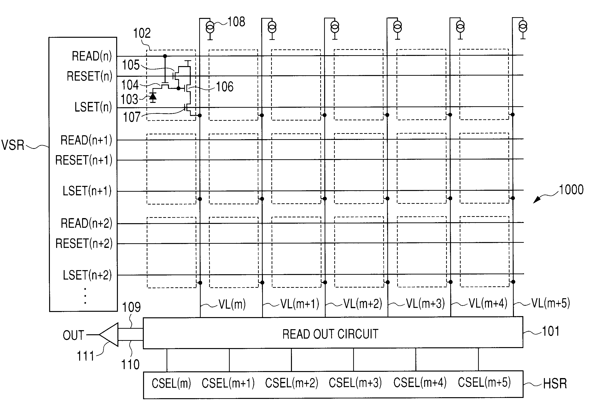
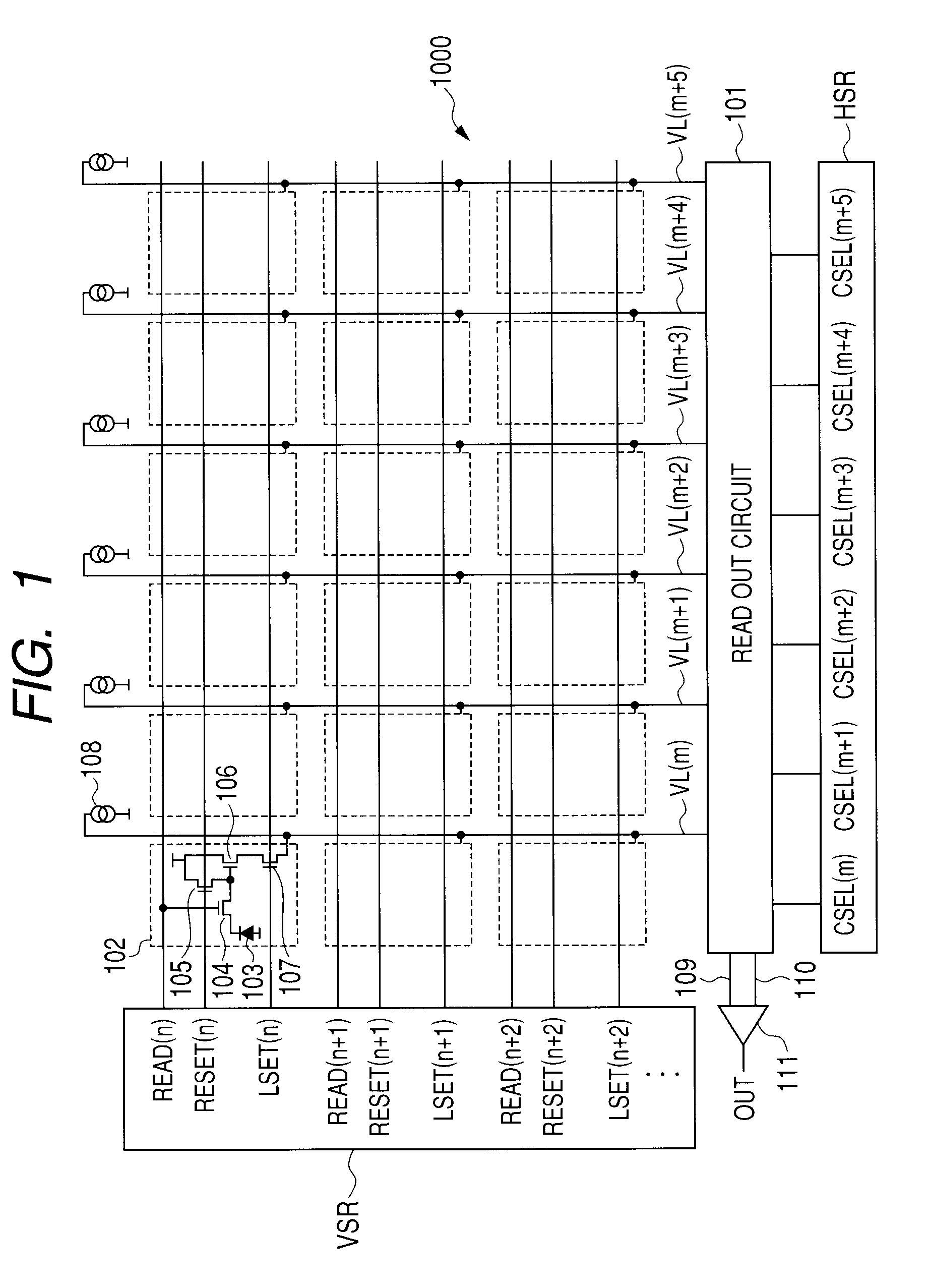
[0037]FIG. 1 is a diagram illustrating an extracted section of nth to n+2th rows and mth to m+5th columns in a configuration of a solid-state imaging apparatus according to the first embodiment of the present invention. To simplify the explanation, it is assumed that the solid-state imaging apparatus is a monochrome solid-state imaging apparatus.

[0038]A solid-state imaging apparatus 1000 includes a pixel array 100, a read out circuit 101 as a read out unit, and an output unit 111. Each of pixels 102 included in the pixel array 100 includes a photodiode 103, a transfer transistor 104, a reset transistor 105, an amplification transistor 106 and a selection transistor 107. The photodiode 103 as a photoelectric conversion unit generates and accumulates charges corresponding to an incident light amount. The transfer transistor 104 as a transfer unit switches conduction and non-conduction between...

second embodiment

[0084]Next, a second embodiment of the present invention is described. In the first embodiment, it is assumed that capacitance values of the first holding capacitors 201 to 206 are equal. Therefore, three pixels to be averaged are treated equally. In the second embodiment, a configuration for performing averaging with weighting taken into account is described.

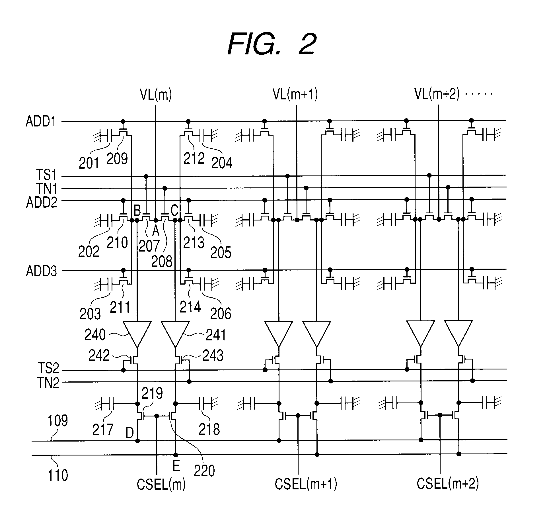
[0085]FIG. 6 is schematic representation of a configuration of a read out circuit according to this embodiment. The read out circuit is different from the read out circuit illustrated in FIG. 2 in that third holding capacitors 202′ and 205′ are added as third holding units. It is assumed that capacitance values of the first holding capacitors 201 to 206 excluding the holding capacitors 202′ and 205′ are equal. Capacitance values of the holding capacitors 202′ and 205′ may be equal to or may be different from the capacitance values of the holding capacitors 201 to 206. The holding capacitor 202 is connected to the node B via a s...

third embodiment

[0091]A third embodiment of the present invention is described with reference to FIG. 7.

[0092]FIG. 7 is a schematic diagram illustrating a configuration of a solid-state imaging apparatus according to this embodiment. It is assumed that the color filters of the Bayer color array illustrated in FIG. 5 are provided. The configuration is different from the configuration illustrated in FIG. 1 in that gate terminals of amplification transistors 106 and 106′ of the pixel 102 in the nth row and the pixel 102′ in the n+2th row are electrically short-circuited. Although not illustrated in the figure, gate terminals are connected in the same manner for the n+1th row and the n+3th row. The same configuration is repeated in the n+4th row and subsequent rows not illustrated in the figure. A read out circuit is that illustrated in FIG. 2.

[0093]FIG. 8 is a diagram illustrating a driving timing example of averaging operation according to this embodiment. Differences from the driving timing illustra...


PUM


Abstract

A solid-state imaging apparatus, an imaging system and a driving method for the solid-state imaging apparatus that can reduce jaggy while increasing speed of operation for reading out signals are provided. The driving method includes a first step of storing one or more signals from the plurality of pixels in each of the plurality of first holding units; a second step of adding the signals from the plurality of pixels stored in the plurality of first holding units; and a third step of outputting the signal stored in the second holding unit, such that at least a part of a period of the first step is overlapped with a period of the third step.

Description

BACKGROUND OF THE INVENTION[0001]1. Field of the Invention[0002]The present invention relates to a solid-state imaging apparatus used for a digital video camera, a digital still camera and an image input apparatus such as an image scanner.[0003]2. Description of the Related Art[0004]In a solid-state imaging apparatus, an increase in speed of readout is requested. There is a technique disclosed in Japanese Patent Application Laid-Open No. 2001-45378 in response to this request. In the technique disclosed in Japanese Patent Application Laid-Open No. 2001-45378, in a pixel array in which plural pixels are arrayed in a matrix form, a signal for driving the pixels is supplied to the pixels in the same row and signals of the pixels are read out via plural column signal lines extending in a direction along columns. Holding units for holding the signals from the pixels are respectively connected to one end and the other end of each of the column signal lines. In parallel to operation for re...

Claims


Application Information

Patent Timeline
Patent Type & Authority Applications(United States)
IPC IPC(8): H04N5/225H04N5/262H04N5/335H04N5/374H04N5/376
CPCH04N5/378H04N5/347H04N25/46H04N25/75
Inventor OGURA, MASANORIKOIZUMI, TORU
Owner CANON KK
Why Eureka
Try Eureka