Film-formation method, method for manufacturing electro-optical device, electro-optical device, and electronic apparatus

a technology of electrooptical devices and film thickness, applied in the field of film formation, can solve the problems of less likely to achieve accurate external shape, less likely to fill in the ink around the edges of partition walls, and less likely to reduce the thickness of film at the external peripheral, and achieve high-tech electronic effects

Inactive Publication Date: 2010-03-11
KATEEVA
View PDF4 Cites 20 Cited by
  • Summary
  • Abstract
  • Description
  • Claims
  • Application Information

AI Technical Summary

Benefits of technology

[0036]According to this electronic apparatus, the shape of the functional film is accurately formed and an electro-optical device having a highly sophisticated functional fil

Problems solved by technology

However, since the entire partition wall is liquid repellent, there is a problem in that it is difficult to fill the ink around the edges of the partition wall because the pixel section formation ink is repelled from the side surface of the partition wall.
Difficulty in filling the ink around the edges of the partition wall results in a situation in which it is less likely that an accurate external shape will be achieved in which the planar shape of the film is formed by the

Method used


Image

  • Film-formation method, method for manufacturing electro-optical device, electro-optical device, and electronic apparatus
  • Film-formation method, method for manufacturing electro-optical device, electro-optical device, and electronic apparatus
  • Film-formation method, method for manufacturing electro-optical device, electro-optical device, and electronic apparatus

Examples


first embodiment

[0064]Described first is a first embodiment as an embodiment of the film-formation method, method for manufacturing an electro-optical device, electro-optical device, and electronic apparatus. The present embodiment will be described using a film-formation method as an example in which a step is used for forming a color element film (filter film), which is an example of a functional film, in the step for manufacturing a color filter of a liquid crystal display device, which is an example of an electro-optical device.

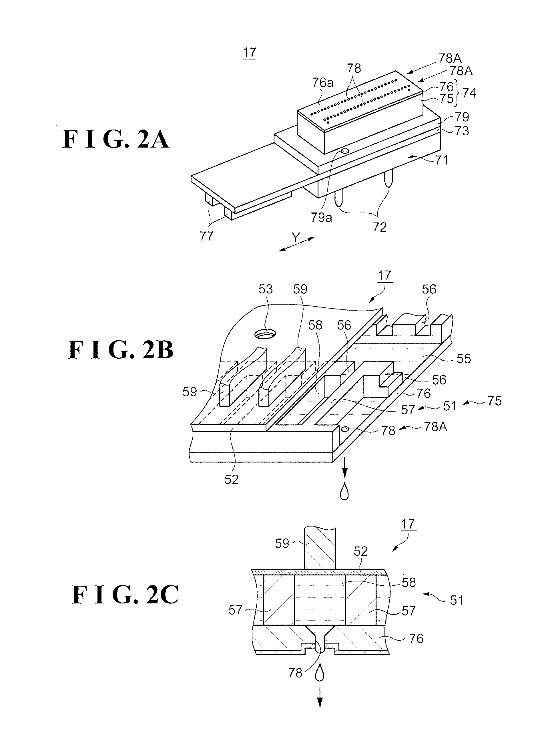
[0065]The droplet discharge method used in the formation of a filter film or another functional film will be described first. The droplet discharge method has an advantage in that a desired amount of material can be deposited with good accuracy in a desired position without wasteful usage of the material. Examples of the discharge technique of the droplet discharge method include an electrification control scheme, a pressurized vibration scheme, an electromechanical conv...

second embodiment

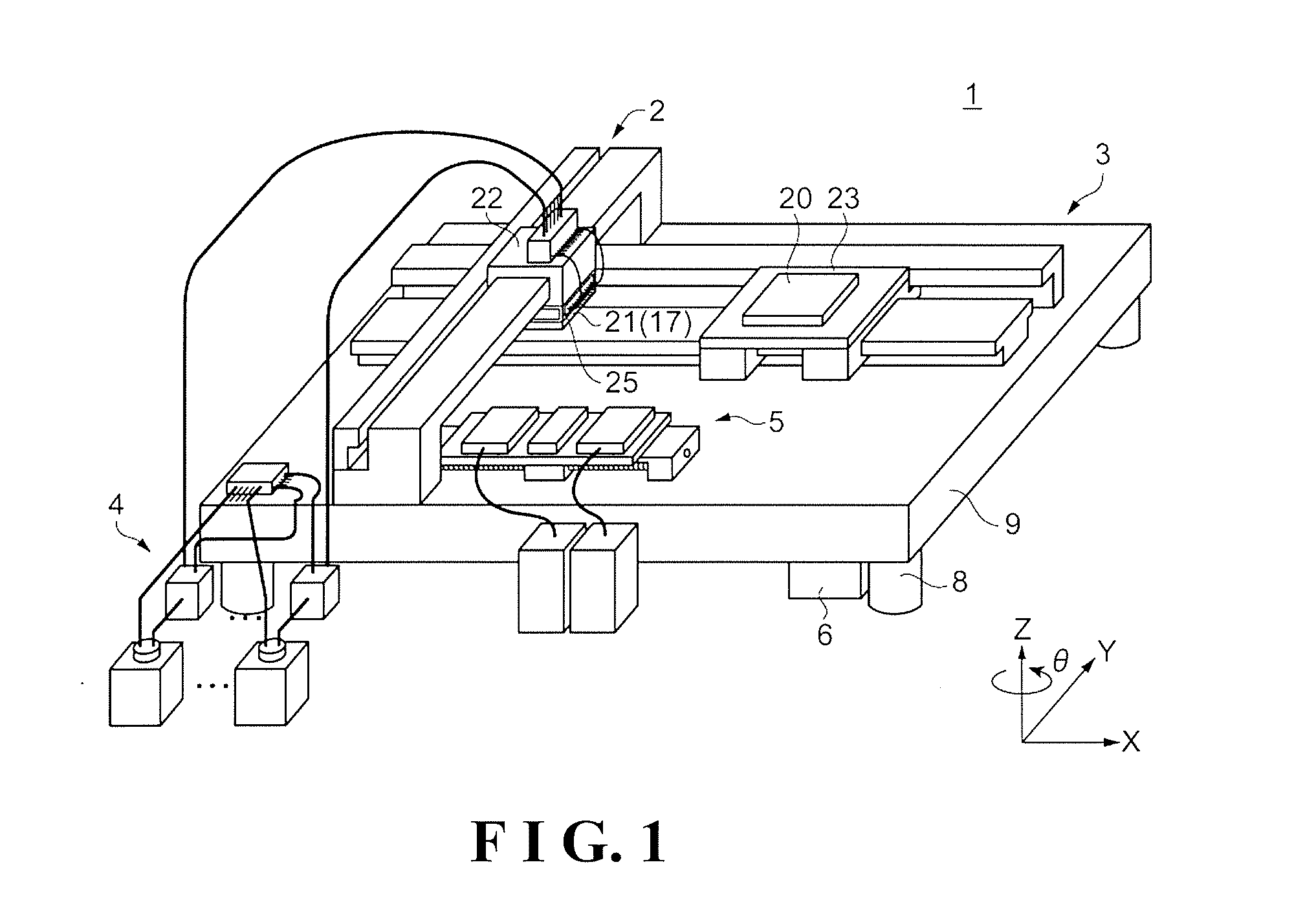
[0135]Described next with reference to the drawings is a second embodiment as an embodiment of the film-formation method, method for manufacturing an electro-optical device, electro-optical device, and electronic apparatus. The present embodiment will be described using a film-formation method as an example in which a step is used for forming a hole-transport layer and a luminescent layer, which are examples of a functional film, in the step for manufacturing an organic EL display device, which is an example of an electro-optical device. The droplet discharge device used in the present embodiment is essentially the same as the droplet discharge device 1 described in the first embodiment.

Configuration of Organic EL Display Device

[0136]First, the configuration of an organic EL display device will be described with reference to FIGS. 11, 12, and 13. FIG. 11 is a schematic front view showing the plan configuration of the organic EL display device. FIG. 12 is a plan view showing the arr...

third embodiment

[0176]Described next with reference to the drawings is a third embodiment as an embodiment of the film-formation method, method for manufacturing an electro-optical device, electro-optical device, and electronic apparatus. The present embodiment will be described in relation to another example of a configuration of the partition walls formed in the step for manufacturing the color filter of a liquid crystal display device described in the first embodiment.


PUM

PropertyMeasurementUnit
Heataaaaaaaaaa
Wettabilityaaaaaaaaaa

Abstract

A film-formation method is a method for depositing a liquid containing a film material to form a film in a prescribed film formation area enclosed by a partition wall on a substrate. The film-formation method includes forming the partition wall using at least in part a wettability-variable material in which wettability with respect to the liquid is variable, depositing the liquid in the film formation area, varying the wettability of the wettability-variable material in the partition wall in a state in which the liquid is disposed within the film formation area so that liquid affinity of the wettability-variable material becomes higher than liquid affinity of the wettability-variable material before the liquid is deposited in the film formation area, and forming the film by solidifying the film material in the liquid.

Description

CROSS-REFERENCE TO RELATED APPLICATIONS[0001]This application claims priority to Japanese Patent Application No. 2008-229469 filed on Sep. 8, 2008. The entire disclosure of Japanese Patent Application No. 2008-229469 is hereby incorporated herein by reference.BACKGROUND[0002]1. Technical Field[0003]The present invention relates to a film-formation method for depositing a film formation material in a film formation region to form a film in the film formation region, a method for manufacturing electro-optical device using the film-formation method, an electro-optical device provided with the film, and an electronic apparatus provided with the electro-optical device.[0004]2. Related Art[0005]There are known conventional techniques for forming a color filter film or another functional film of a color liquid crystal device as an example of an electro-optical device in which droplets of a liquid containing a material of a functional film are discharged and made to land in arbitrary positi...

Claims


Application Information

Patent Timeline
IPC IPC(8): B05D5/12B05D3/00G02F1/00
CPCG02F1/133516H01L51/56H01L51/0005H01L27/3246H10K59/122H10K71/135H10K71/00
Inventor KINOSHITA, TOYOTARO
Owner KATEEVA
Why Eureka
Try Eureka