Method for tuning a work function of high-k metal gate devices

a technology of metal gate device and work function, which is applied in the direction of semiconductor devices, basic electric elements, electrical apparatus, etc., can solve the problems of increasing the complexity of processing and manufacturing ics, affecting device performance, and not being satisfactory in all respects

Inactive Publication Date: 2010-03-18
TAIWAN SEMICON MFG CO LTD
View PDF5 Cites 129 Cited by
  • Summary
  • Abstract
  • Description
  • Claims
  • Application Information

AI Technical Summary

Benefits of technology

[0005]Another one of the broader forms of an embodiment of the invention involves a method of fabricating a semiconductor device. The method includes providing a semiconductor substrate; forming a first transistor and a second transistor in the substrate, the first transistor including a first gate structure, the second transistor including a second gate structure, the first gate structure and the second gate structure each including a high-k dielectric layer formed over the substrate, a barrier layer formed over the high-k dielectric layer, and a dummy poly layer formed over the barrier layer, removing the dummy poly layer from the first and second gate structures thereby forming first and second trenches, respectively, forming a P-type work function metal (P-metal) to partially fill the first and second trenches, removing the P-metal from the first trench, forming a layer of Ti to partially fill the first and second trenches; forming a layer of Al to partially fill the first and second trenches, reflowing the Al layer and Ti layer, and forming a fill metal layer to fill a remainder of the first and second trenches.

Problems solved by technology

However, these advances have increased the complexity of processing and manufacturing ICs and, for these advances to be realized, similar developments in IC processing and manufacturing are needed.
Although this approach has been satisfactory for its intended purpose, it has not been satisfactory in all respects.
For example, the capping layers may decrease carrier mobility, and thus device performance may be adversely affected.

Method used


Image

  • Method for tuning a work function of high-k metal gate devices
  • Method for tuning a work function of high-k metal gate devices
  • Method for tuning a work function of high-k metal gate devices

Examples


Embodiment Construction

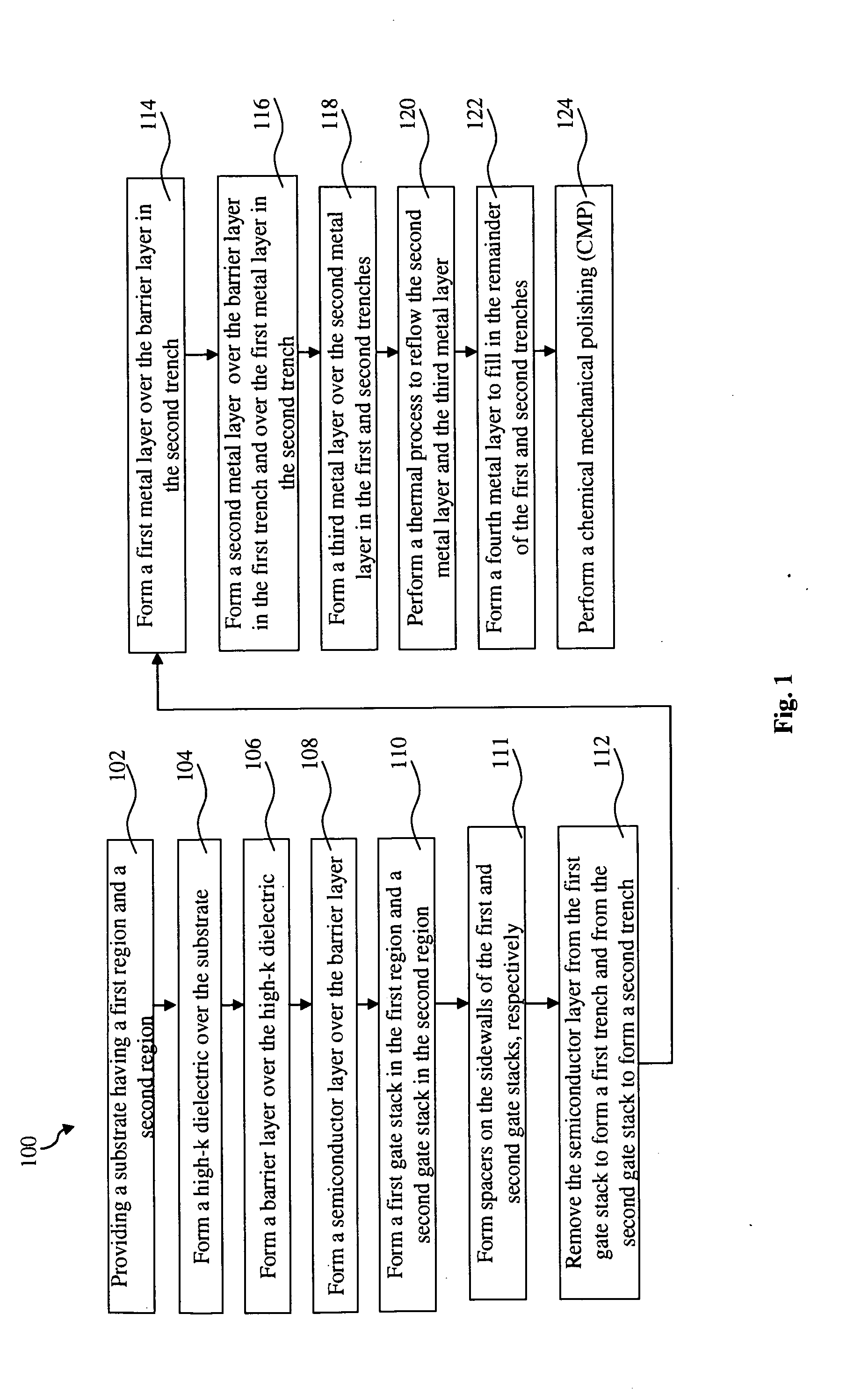
[0010]It is to be understood that the following disclosure provides many different embodiments, or examples, for implementing different features of the invention. Specific examples of components and arrangements are described below to simplify the present disclosure. These are, of course, merely examples and are not intended to be limiting. Moreover, the formation of a first feature over or on a second feature in the description that follows may include embodiments in which the first and second features are formed in direct contact, and may also include embodiments in which additional features may be formed interposing the first and second features, such that the first and second features may not be in direct contact. Various features may be arbitrarily drawn in different scales for simplicity and clarity. In addition, the present disclosure provides examples of a “gate last” metal gate process, however one skilled in the art may recognize applicability to other processes and / or use...


PUM


Abstract

The present disclosure provides a method of fabricating a semiconductor device that includes providing a semiconductor substrate, forming first and second transistors in the substrate, the first transistor having a first gate structure that includes a first dummy gate, the second transistor having a second gate structure that includes a second dummy gate, removing the first and second dummy gates thereby forming a first trench and a second trench, respectively, forming a first metal layer to partially fill in the first and second trenches, removing the first metal layer within the first trench, forming a second metal layer to partially fill in the first and second trenches, forming a third metal layer to partially fill in the first and second trenches, reflowing the second metal layer and the third metal layer, and forming a fourth metal layer to fill in the remainder of the first and second trenches.

Description

PRIORITY DATA[0001]This application claims priority to Provisional Application Ser. No. 61 / 096,659 filed on Sep. 12, 2008, entitled “Method For Tuning A Work Function of High-K Metal Gate Devices,” the entire disclosure of which is incorporated herein by reference.BACKGROUND[0002]The semiconductor integrated circuit (IC) industry has experienced rapid growth. Technological advances in IC materials and design have produced generations of ICs where each generation has smaller and more complex circuits than the previous generation. However, these advances have increased the complexity of processing and manufacturing ICs and, for these advances to be realized, similar developments in IC processing and manufacturing are needed.[0003]In the course of IC evolution, functional density (i.e., the number of interconnected devices per chip area) has generally increased while geometry size (i.e., the smallest component (or line) that can be created using a fabrication process) has decreased. Th...

Claims


Application Information

Patent Timeline
Patent Type & Authority Applications(United States)
IPC IPC(8): H01L21/28
CPCH01L21/28088H01L29/66545H01L29/517H01L21/823842
Inventor YEH, CHIUNG-HANCHUNG, SHENG-CHENTHEI, KONG-BENGCHUANG, HARRY
Owner TAIWAN SEMICON MFG CO LTD
Why Eureka
Try Eureka