Light emitting diode, package structure and manufacturing method thereof

a technology of light emitting diodes and package structures, which is applied in the manufacture of semiconductor/solid-state devices, semiconductor devices, electrical devices, etc., can solve the problems of affecting the the electrodes or the nearby semiconductor layers to be destroyed, and the difference in light emitting efficiency of leds, so as to achieve enhanced light emitting efficiency and light emitting efficiency

Active Publication Date: 2010-03-25
IND TECH RES INST
View PDF11 Cites 75 Cited by
  • Summary
  • Abstract
  • Description
  • Claims
  • Application Information

AI Technical Summary

Benefits of technology

[0011]Due to the above, the present disclosure forms the current distribution modifying pattern in the LED to improve a current distribution in the LED, so that light emitting efficiency and reliability of the LED is enhanced. In

Problems solved by technology

However, in the prior art, since the design of the electrodes in the LED is not of ideal disposition, currents are not uniform when the LED is driven, leading to inferior light emitting efficiencies of the LED.
This problem is especially manifest on the edges of the electrodes, and may caus

Method used


Image

  • Light emitting diode, package structure and manufacturing method thereof
  • Light emitting diode, package structure and manufacturing method thereof
  • Light emitting diode, package structure and manufacturing method thereof

Examples


Embodiment Construction

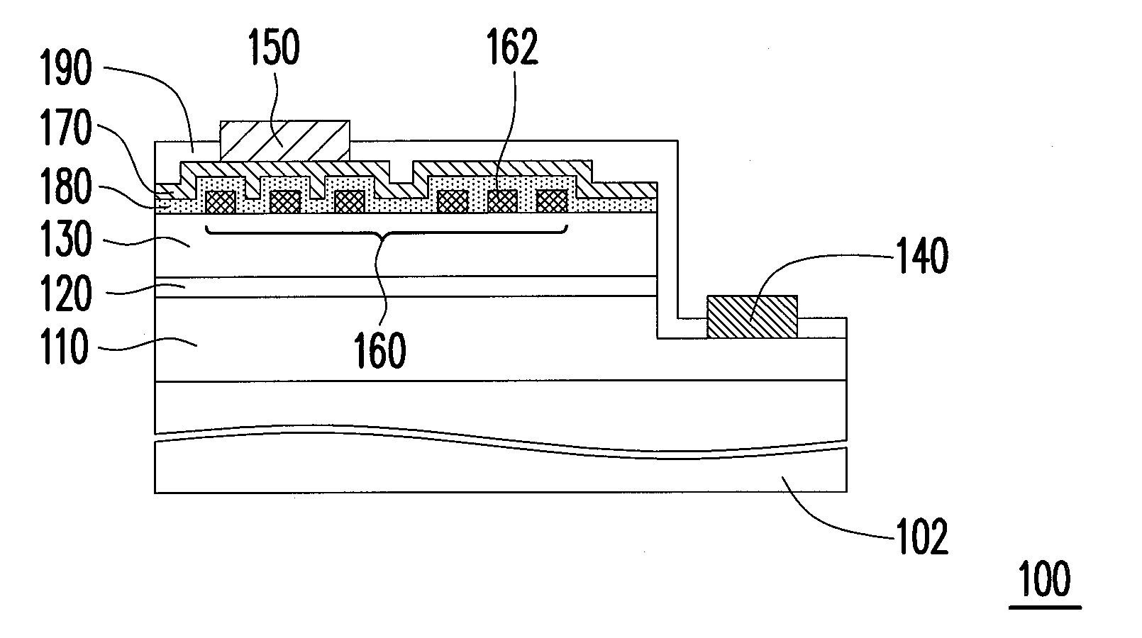
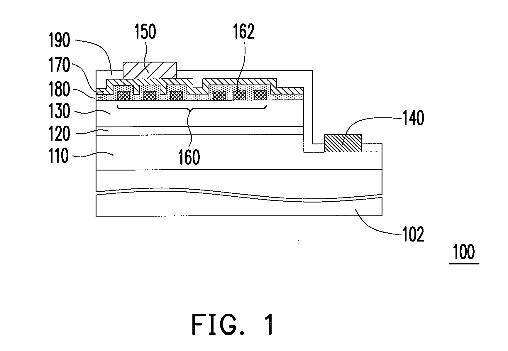
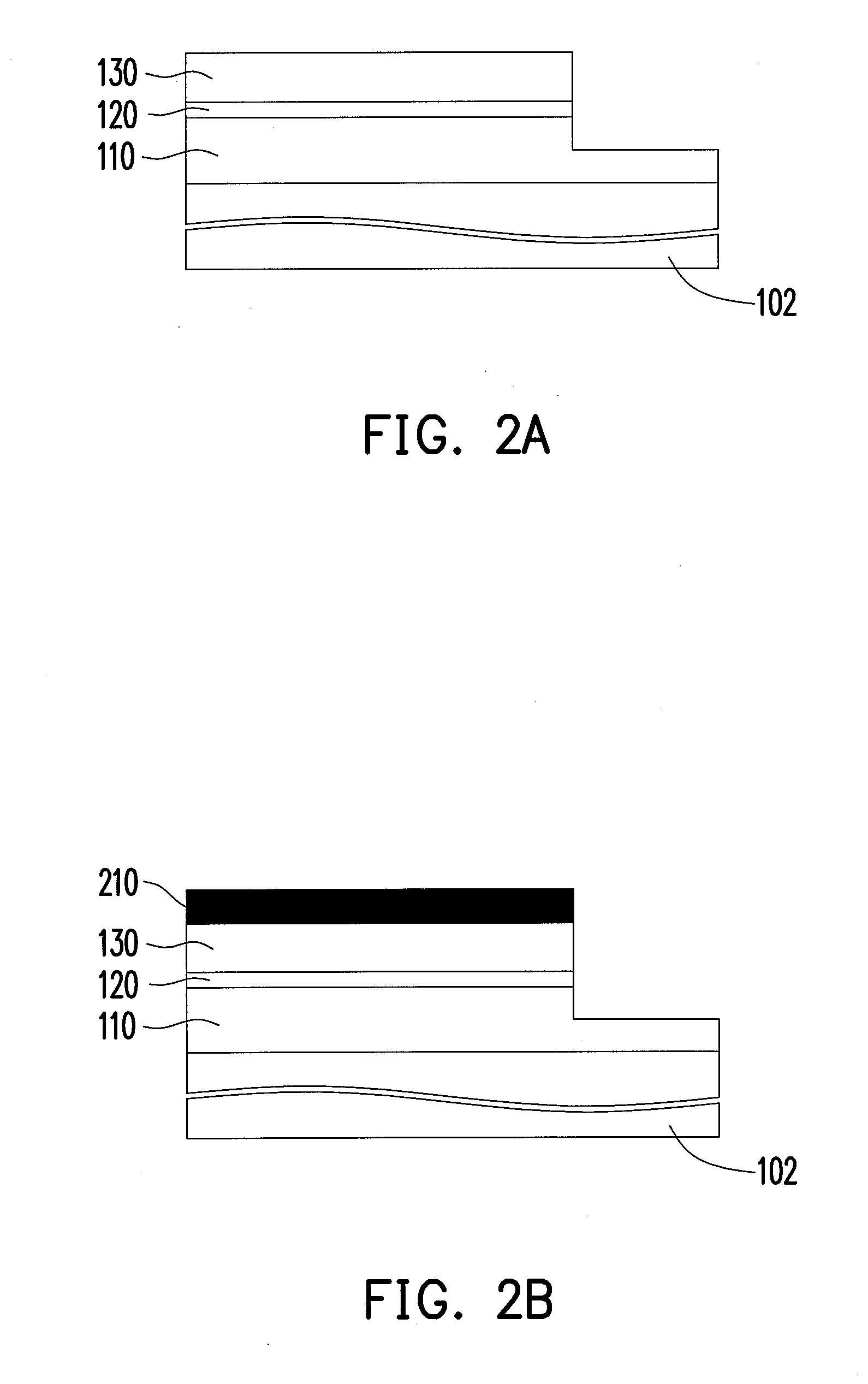
[0025]An LED and a fabricating method thereof in the present disclosure are described below by means of a plurality of embodiment, and a package structure of the LED is further introduced. It should be noted that, detailed structures or steps exemplified according to the following different embodiments can be combined, replaced or omitted under reasonable circumstances to meet different practical needs. A person having ordinary skill in the art should comprehend the spirit and the technical features of the present disclosure after studying the following embodiments, and can perform reasonable modifications and applications without departing from the scope of the present disclosure. In addition, in order to illustrate simply and render the illustrations more comprehensible, the following uses the same reference numerals for similar components and omits repetitive descriptions.

[0026]FIG. 1 is a view illustrating an LED according to an embodiment of the present disclosure. Referring to...


PUM


Abstract

A light emitting diode (LED), a fabricating method thereof, and a package structure thereof are provided. The LED includes a substrate, a first semiconductor layer disposed on the substrate, an active layer disposed on the first semiconductor layer, a second semiconductor layer disposed on the active layer, a current distribution modifying pattern, a first electrode and a second electrode. The active layer and the second semiconductor layer form a mesa structure and expose a part of the first semiconductor layer. The current distribution modifying pattern is disposed on the second semiconductor layer. The first electrode is disposed on and electrically connected to the first semiconductor layer exposed by the mesa structure. The second electrode is disposed on the current distribution modifying pattern and is electrically connected to the second semiconductor layer. The LED has superior light emitting efficiency.

Description

CROSS-REFERENCE TO RELATED APPLICATION[0001]This application claims the priority benefit of Taiwan application serial no. 97136352, filed on Sep. 22, 2008. The entirety of the above-mentioned patent application is hereby incorporated by reference herein and made a part of specification.BACKGROUND OF THE INVENTION[0002]1. Field of the Invention[0003]The present invention relates to a light emitting device and a fabricating method thereof. More specifically, the present invention relates to a light emitting diode (LED), a package structure thereof and a fabricating method thereof.[0004]2. Description of Related Art[0005]An LED is a semiconductor device. A material of light-emitting chips in the LED is generally selected from group III-V chemical elements such as GaP, GaAs, GaN, and other compound semiconductors. The light emitting principle lies in converting electric energy into light. In other words, by applying currents to the compound semiconductors, and through the combinations o...

Claims


Application Information

Patent Timeline
IPC IPC(8): H01L33/00H01L21/02
CPCH01L33/14H01L33/382H01L33/38
Inventor TSAI, YAO-JUNSHEU, JINN-KONGYEN, HSI-HSUANHU, HUNG-LIEH
Owner IND TECH RES INST
Why Eureka
Try Eureka