Substrate-free light emitting diode and fabrication method thereof

a technology of light-emitting diodes and substrates, which is applied in the manufacture of semiconductor/solid-state devices, semiconductor devices, electrical devices, etc., can solve the problems of shortened service life of leds, inability to develop miniaturized displays employing leds, and inflexible led dies, so as to avoid the light shielding effect of electrodes and improve the front light-emitting efficiency of leds

Inactive Publication Date: 2007-07-12
WALSIN LIHWA
View PDF8 Cites 10 Cited by
  • Summary
  • Abstract
  • Description
  • Claims
  • Application Information

AI Technical Summary

Benefits of technology

[0014]One object of the present invention is to provide a method for fabricating a substrate-free light emitting diode (LED). In the substrate-free LED fabricated through this method, a first contact and a conductive supporting layer serving as an electrode are both disposed on the same side of an epitaxy layer, such that the light shielding effect of the electrode may be avoided. Thus, the front light emitting efficiency of the LED may be improved. Furthermore, as for the substrate-free LED provided by the present invention, a thick metal film is employed to serve as both an electrode and an element to support the epitaxy layer, such that the fabricated LED is flexible due to the ductility of the metal. Furthermore, since the LED has no substrate, the whole LED can meet the requirements of miniaturization.

Problems solved by technology

(1) LED dies belong to hard and brittle materials, so the LED dies are not flexible.
However, the heat dissipation of the LED is poor over long time usage, so the service life of the LED is thereby shortened.
(4) Since an LED fabricated through the current process is a bit thick, displays employing such LEDs cannot be developed towards miniaturization.
Furthermore, since the silicon substrate 11 has a certain thickness, the fabricated LED 10 cannot meet the requirements of miniaturization.
Although the above-mentioned two LEDs with different forms have partially solved the problems of heat dissipation and light emitting efficiency through different methods, the structures of the two LEDs still cannot overcome the problems of flexibility and miniaturization.

Method used


Image

  • Substrate-free light emitting diode and fabrication method thereof
  • Substrate-free light emitting diode and fabrication method thereof
  • Substrate-free light emitting diode and fabrication method thereof

Examples


Embodiment Construction

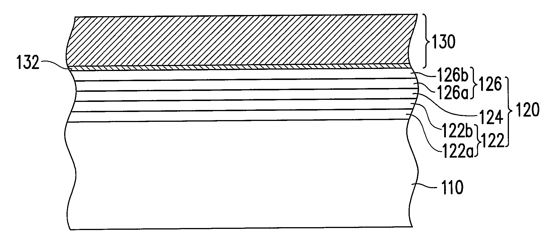
[0044]FIGS. 3A-3F are cross-sectional views of the process of a substrate-free light emitting diode (LED) according to one preferred embodiment of the present invention. First, referring to FIG. 3A, a template substrate 110 is provided. Since the template substrate 110 will be removed once the desired element has been fabricated, all substrates that can grow a favorable epitaxy layer structure can serve as the template substrate 110. The material employed by the template substrate 110 includes semiconductor or non-semiconductor materials, such as, Si, glass, GaAs, GaN, AlGaAs, GaP, SiC, InP, BN, Al2O3, sapphire or AlN.

[0045]Subsequently, referring to FIG. 3A, a first type doped semiconductor layer 122, a light emitting layer 124, and a second type doped semiconductor layer 126 are formed on the template substrate 110 in sequence. Overall, the first type doped semiconductor layer 122, the light emitting layer 124, and the second type doped semiconductor layer 126 can be called collec...


PUM


Abstract

A substrate-free light emitting diode (LED) including an epitaxy layer, a conductive supporting layer, and a first contact pad is provided. The epitaxy layer includes a first type doped semiconductor layer, a light emitting layer, and a second type doped semiconductor layer. The light emitting layer is disposed on the first type doped semiconductor layer, and a portion of the first type doped semiconductor layer is exposed. The second type doped semiconductor layer and the conductive supporting layer are sequentially disposed on the second type doped semiconductor layer. The first contact pad is disposed on the exposed first type doped semiconductor layer and electrically connected thereto. The first contact pad and the conductive supporting layer serving as an electrode are disposed on the same side of the epitaxy layer to avoid the light shielding effects of the electrode to improve the front light emitting efficiency of the LED.

Description

CROSS-REFERENCE TO RELATED APPLICATION[0001]This application claims the priority benefit of Taiwan application serial no. 95101039, filed Jan. 11, 2006. All disclosure of the Taiwan application is incorporated herein by reference.BACKGROUND OF THE INVENTION[0002]1. Field of the Invention[0003]The present invention relates to a light emitting diode (LED) and a fabrication method thereof, and more particularly, to a flexible light emitting diode with preferable front light emitting efficiency and a fabrication method thereof.[0004]2. Description of Related Art[0005]The LED is a semiconductor element that has been widely used in light emitting devices. Generally, the LED chip is made up of III-V group compound semiconductors, such as GaP, GaAs, and GaN. The light emitting principle is to convert electrical energy into light, that is, a current is applied to the compound semiconductor, and by combining electrons with holes, the energy is converted into light so as to achieve the light e...

Claims


Application Information

Patent Timeline
Patent Type & Authority Applications(United States)
IPC IPC(8): H01L33/00H01L21/461
CPCH01L33/0079H01L33/0093
Inventor YANG, CHIEN-CHENGHSIAO, ZHI-CHENGHSIEH, GEN-WEN
Owner WALSIN LIHWA
Why Eureka
Try Eureka