Ink for display device manufacturing and method for manufacturing of the same, method for manufacturing using the same

a technology for display devices and manufacturing methods, applied in the direction of inks, instruments, coatings, etc., can solve the problems of fine metal masks that cannot be dropped, electric conductivity becomes non-uniform, and the size of fine metal masks (fmm) increases, so as to improve the light-emitting efficiency of the display device and high resolution

Active Publication Date: 2015-05-14
LG DISPLAY CO LTD
View PDF9 Cites 12 Cited by
  • Summary
  • Abstract
  • Description
  • Claims
  • Application Information

AI Technical Summary

Benefits of technology

[0010]Embodiments of the present invention provides an ink for display device manufacturing and a method for manufacturing a display device using the same capable of implementing a high resolution and improving a light emitting efficiency of the display device while applying to large-area.

Problems solved by technology

In order to pattern the R, G, and B sub-pixels, the mask is needed, but the size of a fine metal mask (FMM) increases as the area of the substrate increases, such that the problem of dropping the mask may occur.
However, after the ink drops onto the pixel, a coffee ring and pile-up phenomena occurs during the thinning process according to drying, such that the thickness of the thin film becomes non-uniform and when the light emits, the electric conductivity becomes non-uniform, such that a luminance becomes non-uniform. FIG. 1 is a schematic view of the coffee ring phenomenon of the ink and FIG. 2 is a schematic view of a volume decrease phenomenon of the ink.
That is, since the solids due to the evaporation at a portion in which the solids are unsaturated are not precipitated, the precipitation of the solids are not uniform according to the saturation of the ink solvent in all sections the ink is spread, such that the thickness of the ink thin film becomes non-uniform.
Therefore, due to the problems that occur during the drying process of the ink as described above, the light-emitting property of the organic light emitting diode display device deteriorates.

Method used


Image

  • Ink for display device manufacturing and method for manufacturing of the same, method for manufacturing using the same
  • Ink for display device manufacturing and method for manufacturing of the same, method for manufacturing using the same
  • Ink for display device manufacturing and method for manufacturing of the same, method for manufacturing using the same

Examples


example 1

[0051]The solvent was prepared by mixing the 4-methyl anisole as the first solvent, cyclohexyl benzene as the second solvent, and dimethylphthalate as the third solvent in a ratio of 3:5:2 and the iridium compound as the solids was prepared by mixing with 1 wt %.

example 2

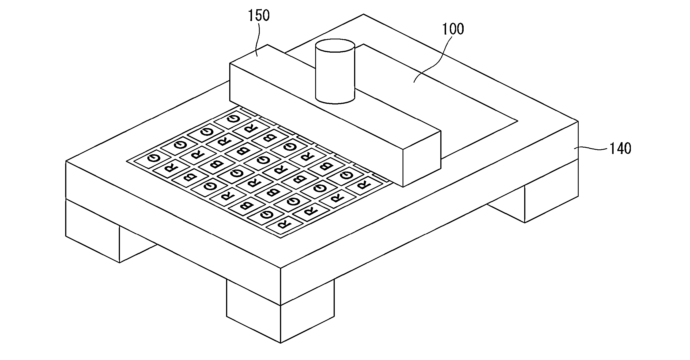
[0055]A hole injection layer (HIL), a hole transport layer (HTL), and a light emitting layer (EML) are formed on the ITO substrate using the ink manufactured according to the example 1 described above. The light emitting layer is formed by the red light emitting layer (EML-R) and the green light emitting layer (EML-G). The organic light emitting diode display device was prepared by forming an electron transport layer (ETL), an electron injection layer (EIL), and an anode using an evaporation method.


PUM

PropertyMeasurementUnit
boiling pointaaaaaaaaaa
voltageaaaaaaaaaa

Abstract

An ink for display device manufacturing, including a solid, a first solvent having a solubility for the solid of 2% or more and a second solvent having a solubility for the solid of 0.5% or less.

Description

[0001]This application claims the priority benefit of Korean Patent Application No. 10-2013-0136235 filed on Nov. 11, 2013, which is incorporated herein by reference for all purposes as if fully set forth herein.BACKGROUND[0002]1. Field of the Invention[0003]The present invention relates to an ink for manufacturing a display device using an inkjet method and a method for manufacturing the display device by using the same.[0004]2. Discussion of the Related Art[0005]Recently a flat panel display (FPD) has become important in accordance with the development of multimedia. Accordingly, various display devices such as a liquid crystal display (LCD) device, a plasma display panel (PDP), a field emission display (FED) device, an organic light emitting diode (OLED) display, and the like have been put to practical use.[0006]Among the display devices, the organic light emitting diode (OLED) display device is a self-light emitting element that emits light by itself while electron-hole pairs di...

Claims


Application Information

Patent Timeline
Patent Type & Authority Applications(United States)
IPC IPC(8): C09D11/36C08K5/01C08K5/101C08K5/13
CPCC09D11/36C08K5/101C08K5/01C08K5/13C09D11/322C09D11/38C09D11/52C09D11/00G02F1/13C09D11/033
Inventor SON, YOUNGTAE
Owner LG DISPLAY CO LTD
Why Eureka
Try Eureka