Method for Fabricating a Vertical Light-Emitting Diode with High Brightness

a technology of light-emitting diodes and manufacturing methods, applied in semiconductor/solid-state device manufacturing, electrical equipment, semiconductor devices, etc., can solve the problems of low efficiency of horizontal light-emitting diodes, and high forward voltage, so as to improve light emission

a technology of light-emitting diodes and manufacturing methods, applied in semiconductor/solid-state device manufacturing, electrical equipment, semiconductor devices, etc., can solve the problems of low efficiency of horizontal light-emitting diodes, and high forward voltage, so as to improve light emission

US20120088318A1Inactive Publication Date: 2012-04-12TEKCORE CO LTD

Image

  • Method for Fabricating a Vertical Light-Emitting Diode with High Brightness
  • Method for Fabricating a Vertical Light-Emitting Diode with High Brightness
  • Method for Fabricating a Vertical Light-Emitting Diode with High Brightness

Examples


Embodiment Construction

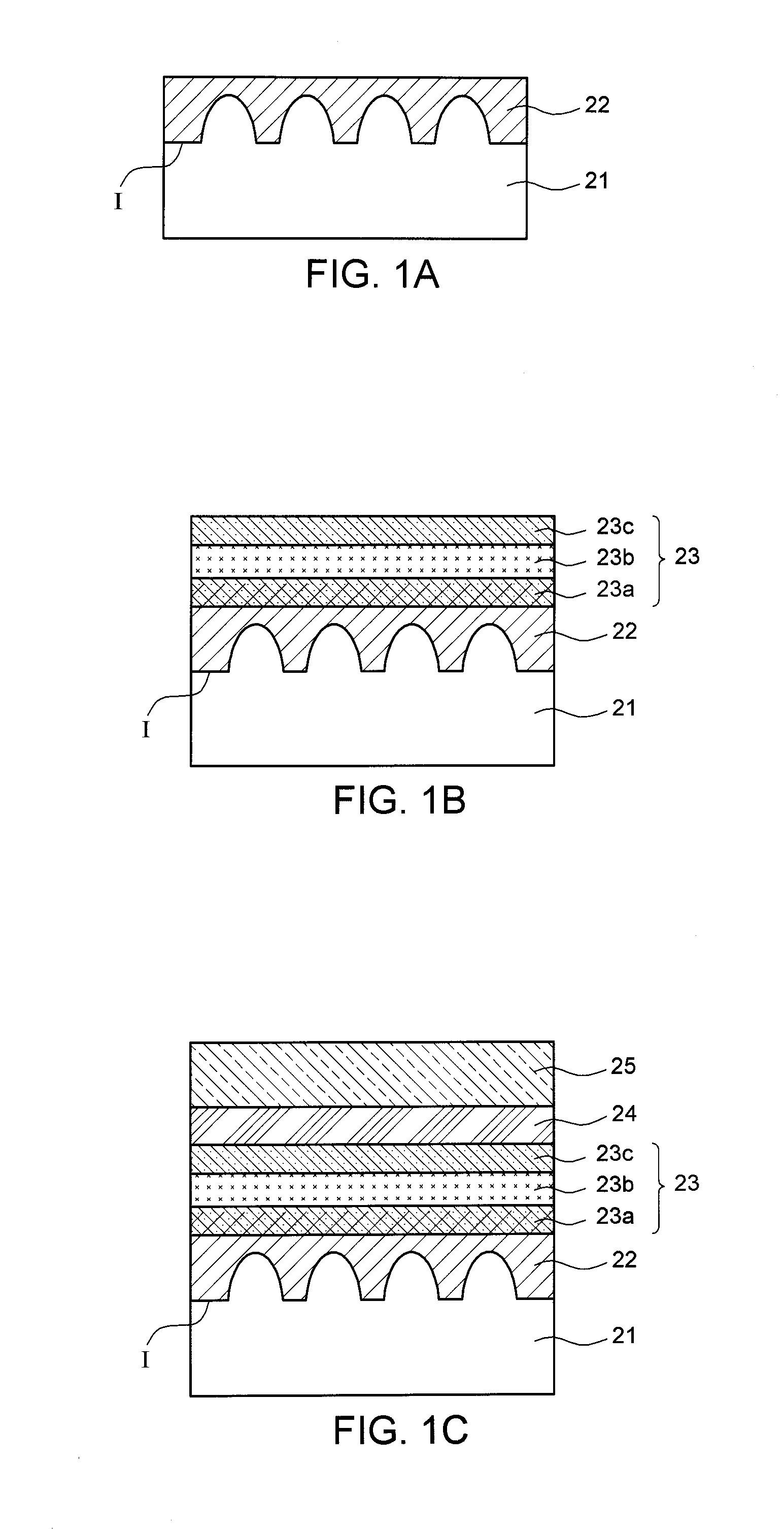
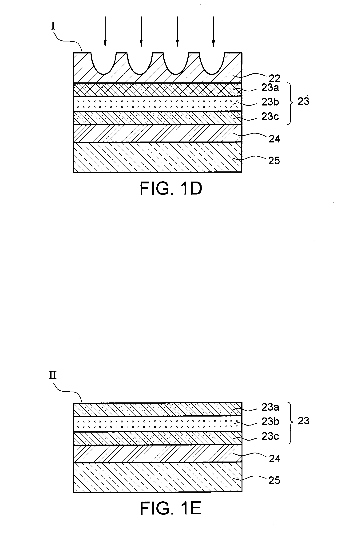
[0013]The present application describes a method for fabricating a vertical light-emitting diode comprised of a stack of multiple epitaxial layers. The stack of the epitaxial layers can be formed on a patterned surface of a sapphire substrate. After the substrate is removed, planarization can be applied on the surface of the stack that was in contact with the patterned surface of the sapphire substrate, and an electrode layer then can be formed on the planarized surface of the stack. A roughening step can also be performed to form uneven patterns on a portion of the second surface for improving light emission through the second surface of the stack. The method described herein can be applied to fabricate various vertical light-emitting diodes, especially vertical light-emitting diodes with high brightness.

[0014]“Group III nitride” as employed herein can refer to a compound that contains nitrogen (N) and a chemical element belonging to the group III of the periodic table such as alum...


PUM


Abstract

A method for fabricating a vertical light-emitting diode comprises forming a stack including a plurality of epitaxial layers on a patterned first substrate, placing a second substrate on the stack, removing the first substrate to expose the first surface, planarizing a first surface of the stack that was in contact with the patterned first substrate and has a pattern corresponding to a pattern provided on the first substrate to form a planarized second surface, and forming a first electrode in contact with a side of the second substrate that is opposite to the stack, and a second electrode in contact with the second surface of the stack. A roughening step can be performed to form uneven surface portions on a region of the second surface for improving light emission through the second surface of the stack.

Description

CROSS-REFERENCE TO RELATED APPLICATION[0001]This application claims priority to Taiwan Patent Application No. 099134805, filed on Oct. 12, 2010.BACKGROUND OF THE INVENTION[0002]1. Field of the Invention[0003]The present invention relates to methods for fabricating a light-emitting diode, and more particularly to a method for fabricating a vertical light-emitting diode that has high brightness.[0004]2. Description of the Related Art[0005]Light-emitting diodes (LED) are widely used in lighting devices and display devices. In a conventional process for fabricating a light-emitting diode, the multilayered light-emitting structure is epitaxially grown on a sapphire substrate. Owing to the low electrical conduction and thermal dissipation of the sapphire substrate, two electrodes may be formed on the same side of the light-emitting diode to form a horizontal type light-emitting diode. However, the lateral light-emitting diode has certain disadvantages, including current crowding effect an...

Claims


Application Information

Patent Timeline
12 Apr 2012
Publication
US20120088318A1
IPC
H01L33/48
CPC
H01L33/007; H01L33/22; H01L33/20; H01L33/0079; H01L33/0093
Inventors
CHANG, HSIANG-SZU; YEH, NIEN-TZE