Light emitting device and method for manufacturing thereof

a technology of light emitting device and manufacturing method, which is applied in the manufacture of electrode systems, electric discharge tubes/lamps, and discharge tubes luminescnet screens, etc., can solve the problems of inability to put the light emitting device to practical use, and low light emitting efficiency, so as to achieve easy confinement, less deterioration of characteristics, and good light emitting efficiency

Inactive Publication Date: 2006-11-02
SEMICON ENERGY LAB CO LTD
View PDF62 Cites 13 Cited by
  • Summary
  • Abstract
  • Description
  • Claims
  • Application Information

AI Technical Summary

Benefits of technology

[0065] The present invention provides a multistacked structure, in which light emitting layers an organic compound and carrier transporting layers including an organic compound are alternately stacked. Since the multistacked structure of the present invention is not a multistacked structure of layers including an organic compound and layers including an inorganic compound, a light emitting device having less deterioration in characteristics and good light emitting efficiency can be obtained without generating stress.
[0066] In the present invention, the light emitting layer and the carrier transporting layer have different polarities form each other, a thickness of the carrier transporting layer is thinner than that of the light emitting layer. In addition, the light emitting layer and the carrier transporting layer have the above described LUMO levels and HOMO levels. Accordingly, carriers having the same polarity as the carrier transporting layer can be easily confined, and carriers having different polarity from the carrier transporting layer move by a tunnel effect. That is, either electrons or holes can be confined, and hence, light emitting efficiency can be improved.
[0067] Further, by providing a buffer layer including an organic compound and a metal compound between an electrode and the carrier transporting layer, flatness can be improved even if the substrate has concavity and convexity. The thickness of the buffer layer may be set to be 60 nm or more. In the present invention, driving voltage is not increased even though the thickness of the buffer layer is increased.
[0068] By implementing the above described manufacturing method, a multistacked structure can be formed. In addition, a light emitting device having less deterioration in characteristic and good light emitting efficiency, in which a film thickness can be easily controlled, can be obtained.

Problems solved by technology

However, there are problems that the reported light emitting devices have low light emitting efficiency and cannot be put to practical use.
The organic light emitting layer and the inorganic compound layer are alternately stacked in the light emitting device disclosed in the patent document 1, and therefore, there is a probability of deteriorating a characteristic due to stress.

Method used


Image

  • Light emitting device and method for manufacturing thereof
  • Light emitting device and method for manufacturing thereof
  • Light emitting device and method for manufacturing thereof

Examples


embodiment mode 1

[0092] An example of the present invention will be described with reference to FIGS. 1 to 4. A case where the carrier transporting layers are hole transporting layers, will be described here.

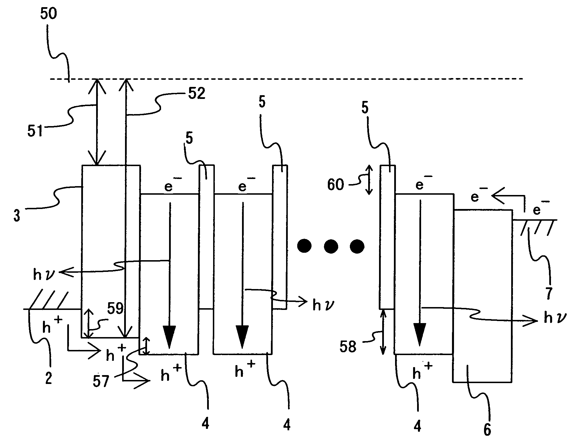
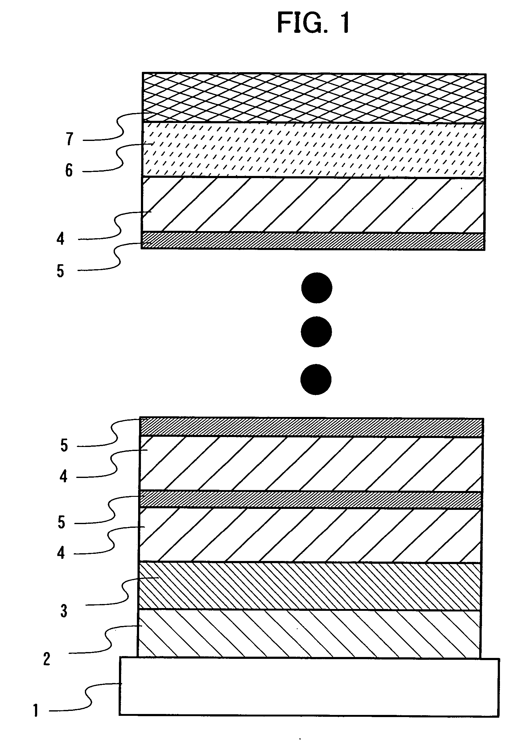
[0093] In a light emitting device shown in FIG. 1, an anode 2; a first hole transporting layer 3; light emitting layers 4 and second hole transporting layers 5 which are repeatedly stacked; an electron transporting layer 6; and a cathode 7 are formed over a substrate 1. A hole injecting layer may be provided between the anode 2 and the first hole transporting layer 3. Further, an electron injecting layer may be provided between the cathode 7 and the electron transporting layer 6. The first and second hole transporting layers may be formed by using the same material, or different materials. Many layers of the second hole transporting layers 5 and the light emitting layers 4 are stacked. A thickness of each of the second hole transporting layers 5 is thinner than a thickness of each of the light ...

embodiment mode 2

[0118] An example of the present invention will be described with reference to FIGS. 1, 2, 5, 6, and the like. A case where the carrier transporting layers are electron transporting layers will be described here.

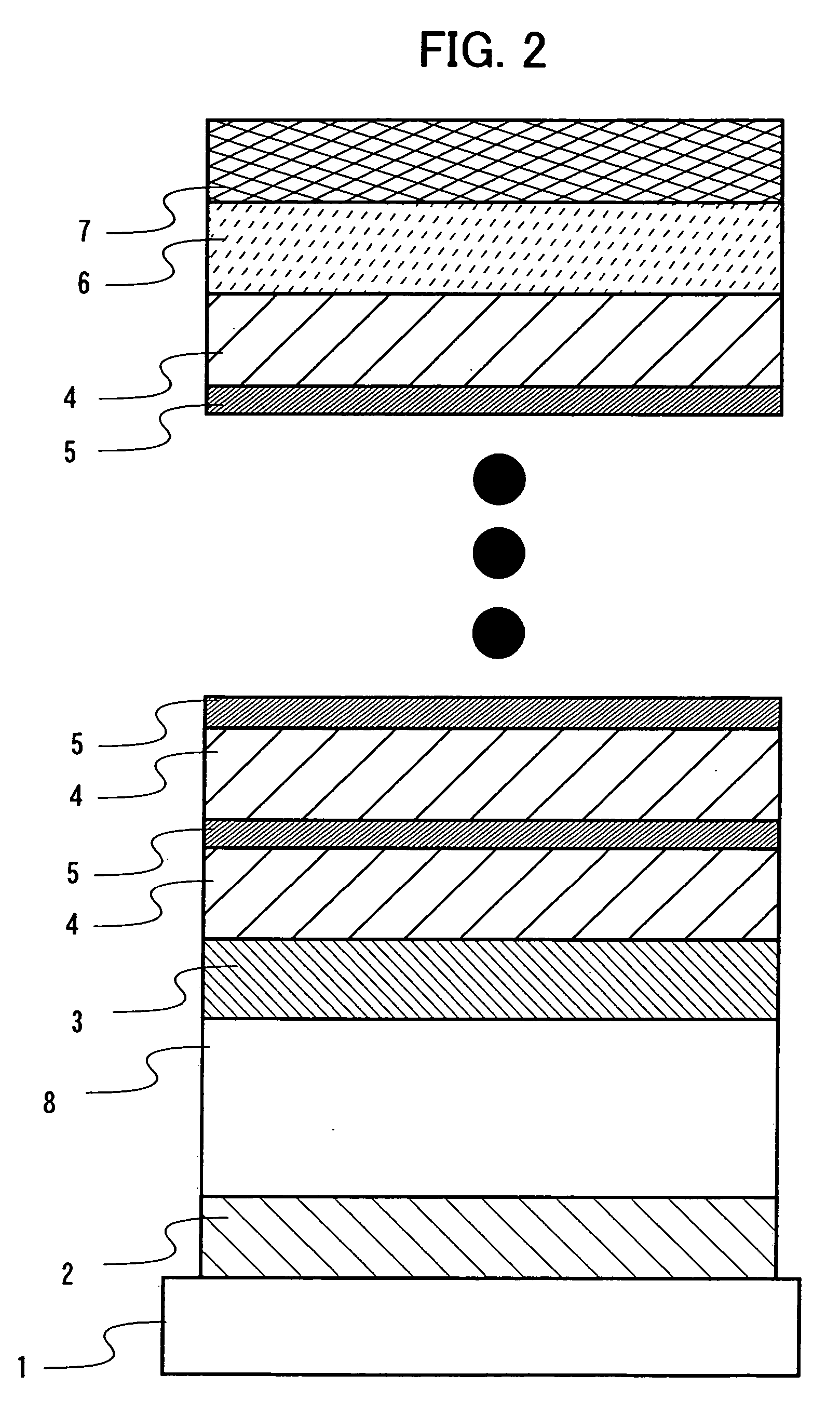
[0119] In a light emitting device shown in FIG. 1, an anode 2; a hole transporting layer 3; light emitting layers 4 and second electron transporting layers 5, which are repeatedly stacked; a first electron transporting layer 6; and a cathode 7 are formed over a substrate 1. A hole injecting layer may be provided between the anode 2 and the hole transporting layer 3. Further, an electron injecting layer may be provided between the cathode 7 and the first electron transporting layer 6. The first and second electron transporting layers may be formed by using the same material, or different materials. Many of the second electron transporting layers 5 and the light emitting layers 4 are stacked. A thickness of each of the second electron transporting layers 5 is thinner than a t...

embodiment mode 3

[0141] An evaporation device used in this embodiment mode and a method for manufacturing a multistacked structure described in Embodiment Modes 1 and 2 by using the evaporation device, will be described with reference to FIG. 7, FIGS. 8A and 8B, FIG. 9, FIG. 10, FIGS. 11A and 11B, FIGS. 12A and 12B, and FIGS. 13A and 13B.

[0142] In the evaporation device used in this embodiment mode, a treatment chamber 1001 in which a target matter is subjected to evaporation treatment, and a transferring chamber 1002 are provided. The target matter is transferred to the treatment chamber 1001 through the transferring chamber 1002. The transferring chamber 1002 is provided with an arm 1003 for moving the target matter (FIG. 7).

[0143] As shown in FIGS. 8A and 8B, in the treatment chamber 1001, a fixing portion 100 for fixing a substrate 101, which is a target matter, an evaporation source 102 filled with a light emitting material, and an evaporation source 103 filled with a carrier transporting mat...


PUM


Abstract

An object of the present invention is to provide a light emitting device including an organic light emitting layer and an organic compound and having high light emitting efficient along with less deterioration in characteristics. In the light emitting device, an anode, a cathode facing the anode, light emitting layers each comprising an organic compound and being provided between the anode and the cathode, and carrier transporting layers each comprising an organic compound, are provided over a substrate. Each of the light emitting layers and each of the carrier transporting layers are alternately stacked. A thickness of each of the carrier transporting layers is thinner than that of each of the light emitting layers. When each of the carrier transporting layers is a hole transporting layer, each of the light emitting layers has an electron transporting property. When each of the carrier transporting layers is an electron transporting layer, each of the light emitting layers has a hole transporting property.

Description

BACKGROUND OF THE INVENTION [0001] 1. Field of the Invention [0002] The present invention relates to a light emitting device used for a display and the like, and a method for manufacturing thereof. [0003] 2. Description of the Related Art [0004] In recent years, with advance of an information society, needs of a display device, which requires lesser power and is thinner than a conventional CRT, have been increased. As such the display, a liquid crystal display and a plasma display can be given, and these displays have already been put to practical use. [0005] In these days, development of a light emitting device utilizing an organic compound has been carried out so as to realize more reduction in power consumption and more vivid full-colors than the liquid crystal display and the plasma display. In this light emitting device, electrodes (an anode and a cathode) are attached to both surfaces of a solid thin film formed using an organic compound, which emits strong fluorescence or pho...

Claims


Application Information

Patent Timeline
Patent Type & Authority Applications(United States)
IPC IPC(8): H01L51/52H01L51/56H05B33/12
CPCH01L51/5012H01L2251/558Y10T428/24967Y10T428/24942Y10T428/2495H10K50/11H10K2102/351
Inventor NOMURA, RYOJIKATO, KAORUYOSHIMOTO, SATOSHIYAMAZAKI, SHUNPEI
Owner SEMICON ENERGY LAB CO LTD
Why Eureka
Try Eureka