Light emitting diode device, and manufacture and use thereof

a technology of light-emitting diodes and diodes, which is applied in the manufacture of semiconductor/solid-state devices, semiconductor devices, electrical devices, etc., can solve the problems of unnecessarily bulky led packaging, and achieve the effect of enhancing light-emitting

Active Publication Date: 2008-03-13
HONG KONG APPLIED SCI & TECH RES INST
View PDF35 Cites 14 Cited by
  • Summary
  • Abstract
  • Description
  • Claims
  • Application Information

AI Technical Summary

Benefits of technology

[0005]According to a first aspect of the present invention, there is provided a light emitting diode device. The light emitting diode device includes a multi-layer stack of materials including a p-layer, a n-layer, and a light generating region for emission of light in a primary emission direction towards one of the p- and n-layers; a substantially transparent layer located at or adjacent said one of the p- and n-layers, having a first surface facing said one of the p- and n-layers and an opposed second surface; and a reflective surface formed at or adjacent the second surface of the transparent layer for directing at least a portion of the emitted light in a direction away from the primary emission direction so as to enhance light emission from a side of the light emitting diode device.

Problems solved by technology

Conventionally, complicated optical designs have been adopted in the packaging of the LED, which may make the LED packaging unnecessarily bulky.

Method used


Image

  • Light emitting diode device, and manufacture and use thereof
  • Light emitting diode device, and manufacture and use thereof
  • Light emitting diode device, and manufacture and use thereof

Examples


embodiment 400

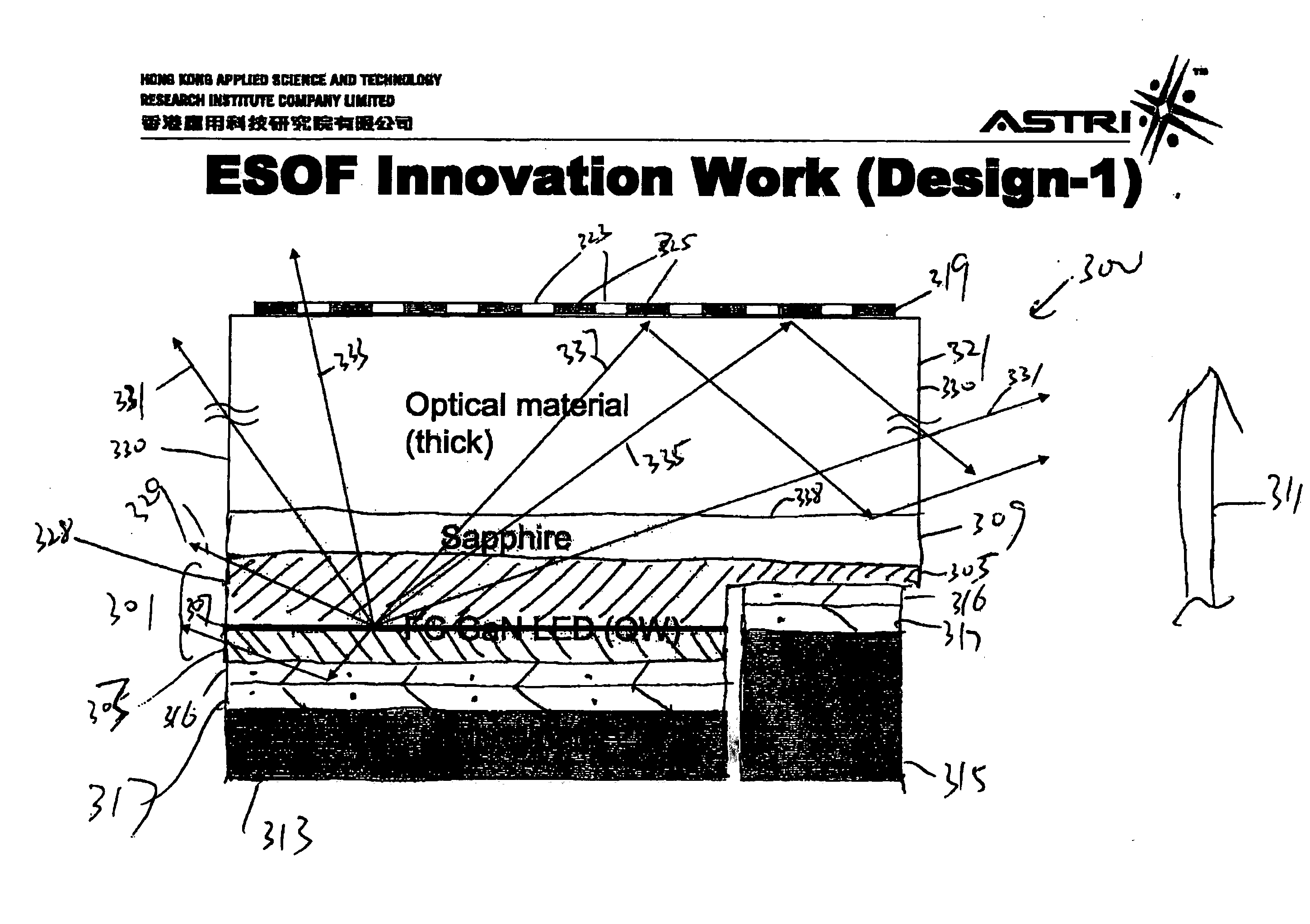
[0041]In FIG. 4, a second flip-chip LED device embodiment 400 further includes a 2-dimensional photonic crystal structure 401 formed between the substrate 403 and the transparent layer 405 for extracting lights from the substrate 403 towards the transparent layer 405, and the 2-dimensional photonic crystal structure 401 has a photonic band gap covering at least a segment of a wavelength range of the lights emitted by p-n junction 407. The fabrication and application of such a 2-dimensional photonic crystal structure is described in detail in a co-pending US patent application entitled “Semiconductor Light Emitting Device” and filed by Yan Hung et al., the contents of which are herein incorporated by reference.

embodiment 500

[0042]In a third flip-chip LED device embodiment 500 illustrated in FIG. 5, the reflective mirrors 503 on the reflective layer 501 have a U-shape or a convex shape. The convex shaped reflective mirrors can be formed by firstly creating a plurality of concave shaped recesses 504 on the top surface 506 of the transparent layer 509 and then depositing a layer of reflective material onto each recess 504.

[0043]As compared to the flat reflective mirrors shown in FIGS. 3a and 4, the convex-shaped reflective mirror design may reduce light reflections towards the p-n junction and therefore may increase light emissions out of the LED device. Furthermore, such an LED device may achieve more complicated and / or better controlled light illumination field patterns by adjusting the size and dimensions of the convex-shaped reflective mirrors 503, the size of the apertures 507 between the reflective mirrors 503, and the thickness of the transparent layer 509.

[0044]FIG. 6a illustrates an exemplary emb...


PUM


Abstract

A light emitting diode device includes a multi-layer stack of materials including a p-layer, a n-layer, and a light generating region for emission of light in a primary emission direction towards one of the p- and n-layers; a substantially transparent layer located at or adjacent said one of the p- and n-layers, having a first surface facing said one of the p- and n-layers and an opposed second surface; and a reflective surface formed at or adjacent the second surface of the transparent layer for directing at least a portion of the emitted light in a direction away from the primary emission direction so as to enhance light emission from a side of the light emitting diode device.

Description

FIELD OF THE INVENTION[0001]The invention relates to light emitting diodes (LEDs) and more particularly to LEDs having enhanced side emission.BACKGROUND OF THE INVENTION[0002]LEDs are semiconductor devices that emit lights when an electrical current is supplied thereto. As shown in FIGS. 1a and 1b, typically, an LED 100 is formed of multiple layers of materials having a layer of p-doped material or p-type semiconductor layer (“p-layer”) 101, a layer of n-doped material or an n-type semiconductor layer (“n-layer”) 103, and a light generating region or p-n junction 105. When powered, the p-n junction emits lights in a primary direction 107 towards one of the p- and n-layers creating a field of illumination 109 roughly along a longitudinal axis parallel to the direction 107.[0003]In certain applications of LEDs, for example in a backlight illumination system, it may be desirable to convert the LED's light illumination field 109 into a “bat-wing” light illumination field 201 as illustra...

Claims


Application Information

Patent Timeline
Patent Type & Authority Applications(United States)
IPC IPC(8): H01L33/00H01L21/00H01L33/20H01L33/44H01L33/46
CPCH01L33/20H01L2933/0083H01L33/46H01L33/44
Inventor CHIU, KUO ANFENG, JIANPENG, HUAIJUNCHU, HUNG-SHENZHENG, SHENGMEI
Owner HONG KONG APPLIED SCI & TECH RES INST
Why Eureka
Try Eureka