Organic light-emitting diode (OLED) display panel and manufacturing method

a technology of light-emitting diodes and display panels, applied in the field of display panels, can solve problems such as degrading the display performance of oled display panels

Active Publication Date: 2017-08-31
WUHAN TIANMA MICRO ELECTRONICS CO LTD +1
View PDF7 Cites 10 Cited by
  • Summary
  • Abstract
  • Description
  • Claims
  • Application Information

AI Technical Summary

Benefits of technology

[0022]A micro-cavity structure may be formed between the first electrode 2 and the second electrode 6. The effects of reflection, total reflection, interference, diffraction, or scattering on the interface of the discontinuous refractive index in the micro-cavity structure may be adopted to confine the emitted light within a relatively small wavelength band. The cavity length and the thicknesses of the layers of the micro-cavity may be designed, such that the wavelength center of the emitted light may be configured to be located near the antinodes of the standing wave field. Thus, the coupling efficiency of the radiation dipole and the electric field inside the micro-cavity may be increased, and the light-emitting efficiency (i.e., luminous efficiency) and brightness of the device may be improved.

Problems solved by technology

However, adjusting the cavity length of the micro-cavity structure by the thickness of the hole transport layer may cause serious crosstalk and degrade the display performance of the OLED display panel.

Method used


Image

  • Organic light-emitting diode (OLED) display panel and manufacturing method
  • Organic light-emitting diode (OLED) display panel and manufacturing method
  • Organic light-emitting diode (OLED) display panel and manufacturing method

Examples


Embodiment Construction

[0014]Reference will now be made in detail to exemplary embodiments of the disclosure, which are illustrated in the accompanying drawings. Wherever possible, the same reference numbers will be used throughout the drawings to refer to the same or like parts. It should be understood that the exemplary embodiments described herein are only intended to illustrate and explain the present invention and not to limit the present invention. In addition, it should also be noted that, for ease of description, only part, but not all, of the structures associated with the present invention are shown in the accompanying drawings.

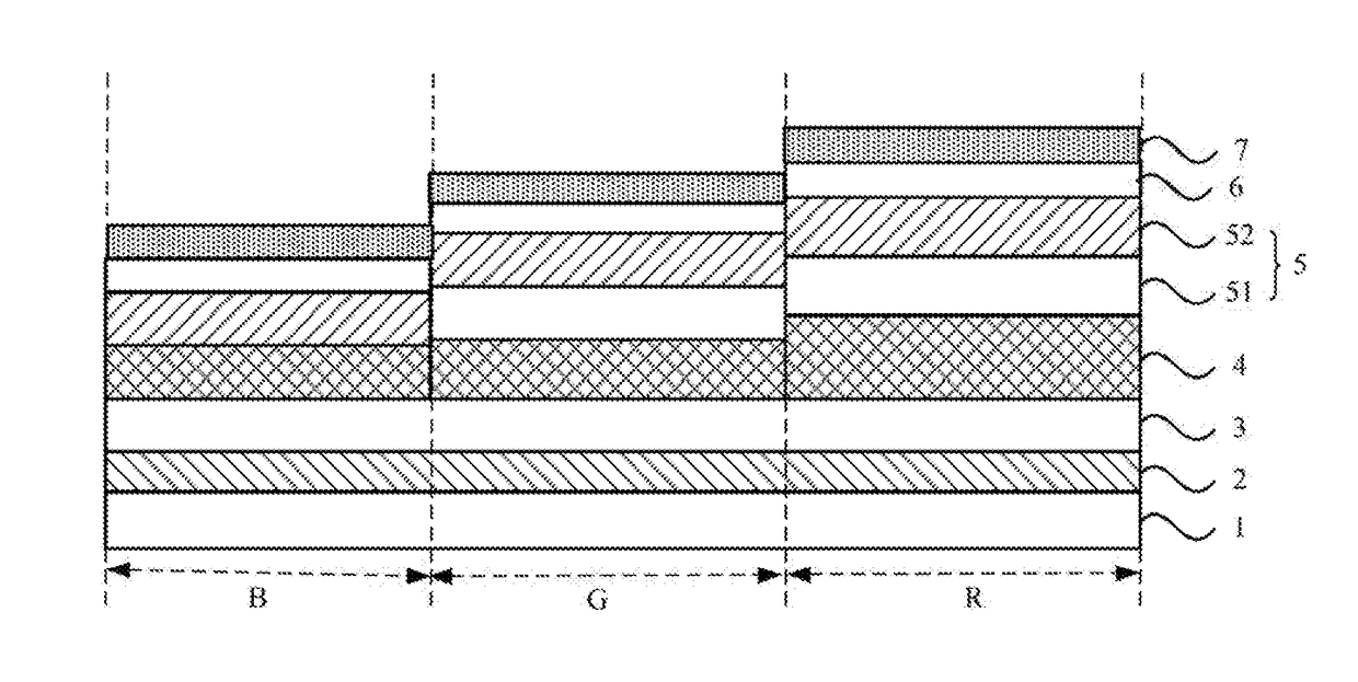
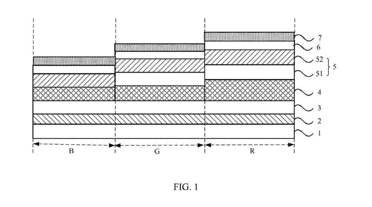
[0015]The present disclosure provides an OLED display panel, comprising a plurality of pixel regions disposed on a substrate and emitting light in different colors. Each pixel region may comprise a first electrode, a first auxiliary light-emitting layer, a light-emitting layer, a second auxiliary light-emitting layer, and a second electrode, which are disposed facing away...


PUM


Abstract

The present disclosure provides an OLED display panel, comprising a substrate and a plurality of pixel regions disposed on the substrate and emitting light in different colors. A pixel region includes a first electrode, a first auxiliary light-emitting layer, a light-emitting layer, a second auxiliary light-emitting layer, and a second electrode. A micro-cavity structure is formed between the first electrode and the second electrode. The second auxiliary light-emitting layer includes at least a first sub-auxiliary light-emitting layer. The second auxiliary light-emitting layer corresponding to the pixel regions emitting light in at least one color also includes a second sub-auxiliary light-emitting layer. At least one of the first sub-auxiliary light-emitting layer and the second sub-auxiliary light-emitting layer is made of at least a first electron-type material. The second sub-auxiliary light-emitting layer has a zero-field electron mobility greater than or equal to a pre-determined threshold.

Description

CROSS-REFERENCES TO RELATED APPLICATIONS[0001]This application claims the priority of Chinese Patent Application No. CN201610986284.5, filed on Nov. 9, 2016, the entire contents of which are incorporated herein by reference.FIELD OF THE DISCLOSURE[0002]The present disclosure generally relates to the display technology and, more particularly, relates to an OLED display panel and a manufacturing method thereof.BACKGROUND[0003]Organic light-emitting diodes (OLEDs) are also known as organic electroluminescent device. Driven by an electric field, the light-emitting material in the OLED emits light through carrier injection and recombination. Compared to liquid crystal display (LCD) devices, OLED devices are lighter and thinner, and have wider viewing angles and higher contrast. Thus, the OLED devices are becoming more and more popular.[0004]In an existing OLED display panel, an optical resonant micro-cavity (also referred to as a micro-cavity structure) is adopted to adjust light-emittin...

Claims


Application Information

Patent Timeline
Patent Type & Authority Applications(United States)
IPC IPC(8): H01L27/32H01L51/56H01L51/00H01L51/52
CPCH01L27/3216H01L51/0072H01L51/56H01L51/5203H10K59/35H10K50/155H10K50/165H10K50/852H10K71/00H10K85/6572H10K50/11H10K2101/00
Inventor HE, WEICHENG, SHUANGNIU, JINGHUAWANG, XIANGCHENGHAMADA, YUJILIU, CHEN
Owner WUHAN TIANMA MICRO ELECTRONICS CO LTD
Why Eureka
Try Eureka