Light-emitting device and lighting device including the same

a technology of light-emitting devices and lighting devices, which is applied in the direction of semiconductor devices, basic electric elements, electrical appliances, etc., can solve the problems of low color rendering index (cri) of white light using leds, phosphor configuration, and wavelength bands to be used, so as to improve the color rendering index (cri) of white light, improve the efficiency of hole injection into an electron blocking layer (ebl), and improve the effect of light properties

Active Publication Date: 2018-12-06
SUZHOU LEKIN SEMICON CO LTD
View PDF17 Cites 10 Cited by
  • Summary
  • Abstract
  • Description
  • Claims
  • Application Information

AI Technical Summary

Benefits of technology

[0023]According to the embodiments, a color rendering index (CRI) of white light can be improved. Particularly, a CRI of R12 can be improved even without an additional phosphor.
[0024]In addition, efficiency of hole injection into an electron blocking layer (EBL) can be improved. Accordingly, a problem in that light properties are lowered can be improved even when a size of a recess is increased.
[0025]In addition, since holes can be injected into a lower portion of an active layer, light emitting efficiency can be improved. Accordingly, a droop phenomenon can be reduced.
[0026]Various useful merits and effects of the present invention are not limited to the above effects and can be more easily understood from specific embodiments of the present invention which will be described below.

Problems solved by technology

However, white light using an LED has a problem of a low color rendering index (CRI).
To solve this problem, there is a problem in that a phosphor configured to be excited in various wavelength bands has to be used.

Method used


Image

  • Light-emitting device and lighting device including the same
  • Light-emitting device and lighting device including the same
  • Light-emitting device and lighting device including the same

Examples


Embodiment Construction

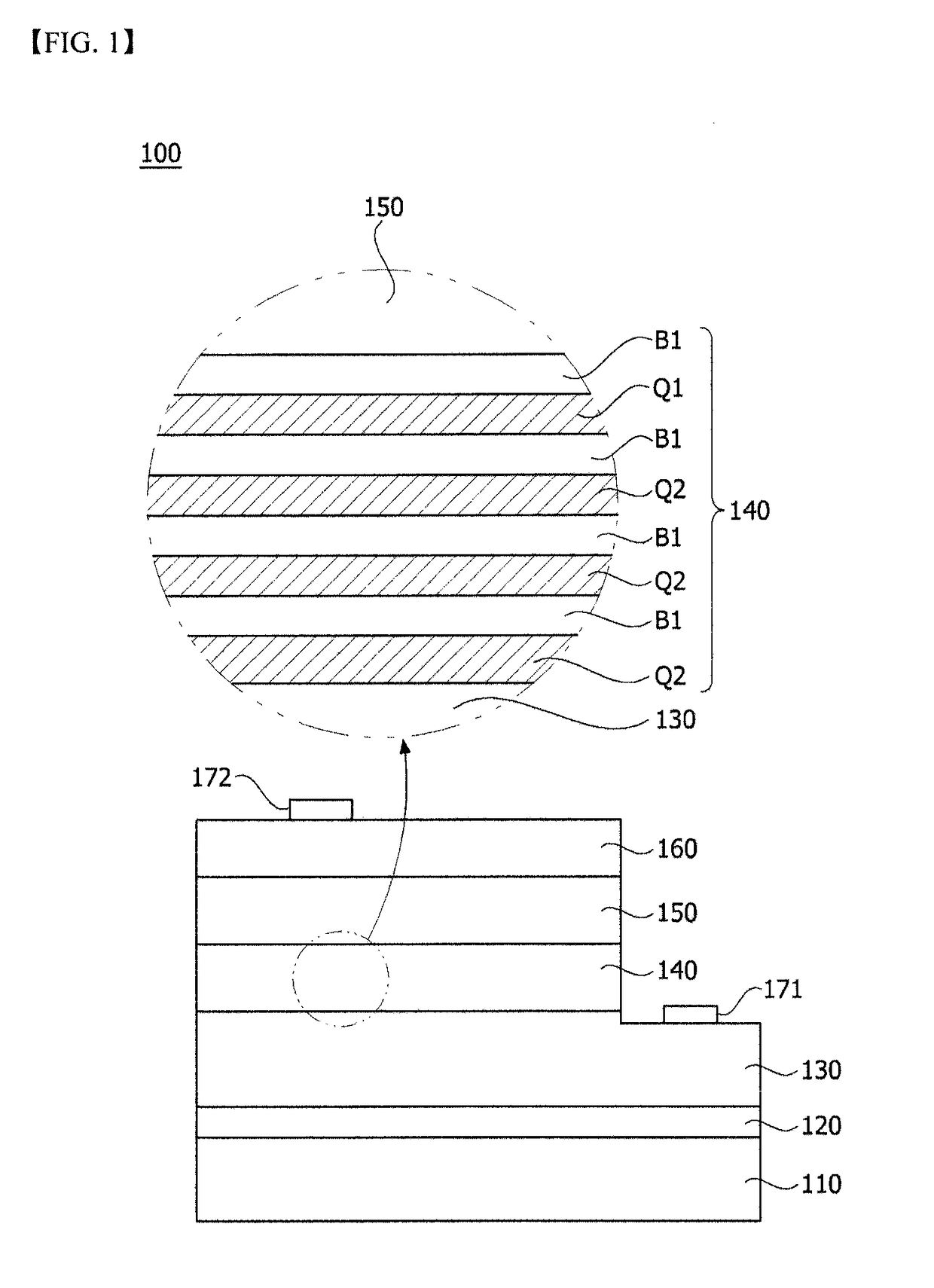
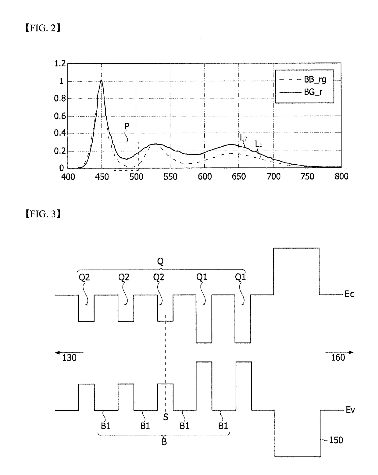
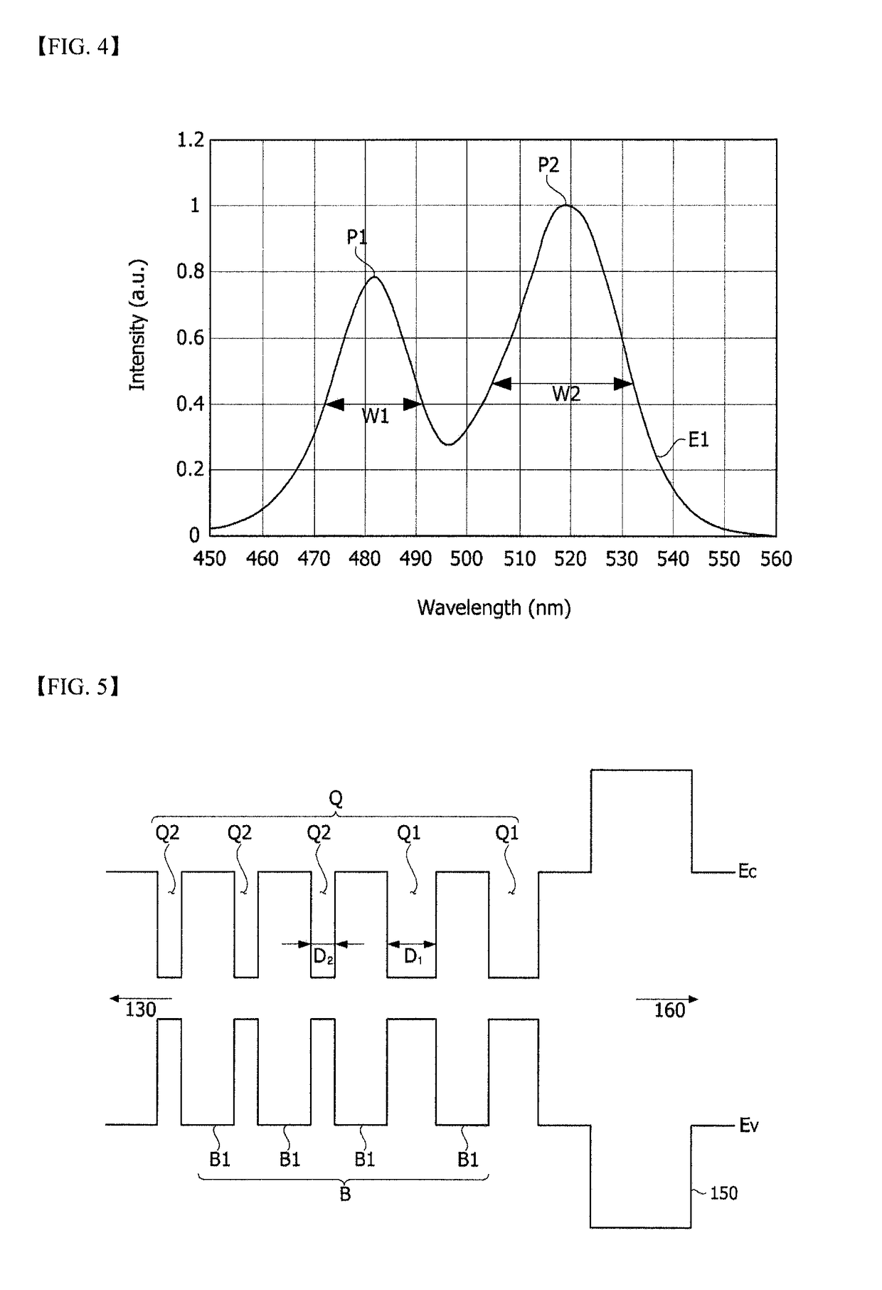
[0044]As the present invention allows for various changes and numerous embodiments, exemplary embodiments will be illustrated in the drawings and described in detail in the written description. However, this is not intended to limit the embodiments of the present invention to particular modes of practice, and it is to be appreciated that all changes, equivalents, and substitutes that do not depart from the spirit and technical scope of the embodiments are encompassed in the embodiments.

[0045]It will be understood that, although the terms “first,”“second,” etc. may be used herein to describe various elements, the elements should not be limited by the terms. The terms are only used to distinguish one element from another. For example, a first element could be termed a second element, and, similarly, a second element could be termed a first element, without departing from the scope of the present invention. As used herein, the term “and / or” includes any and all combinations of one or m...


PUM


Abstract

Disclosed in one embodiment is a light-emitting device comprising: a first conductive semiconductor layer; an active layer arranged on the first conductive semiconductor layer, and including a plurality of first recesses; an EBL arranged on the active layer, and including a plurality of second recesses arranged on the first recesses; and a second conductive semiconductor layer arranged on the EBL, wherein the ratio of a first area doping concentration and a second recess doping concentration is from 1:0.8 to 1:1, the active layer emits first light and second light, the first light has a peak in a wavelength of 450 nm to 499 nm, and the second light has a peak in a wavelength of 500 nm to 550 nm.

Description

TECHNICAL FIELD[0001]The present invention relates to a light emitting device (LED) and a lighting device including the same.BACKGROUND ART[0002]Light emitting devices (LEDs) are compound semiconductor elements configured to convert electrical energy into light energy and may develop various colors by adjusting a composition ratio of a compound semiconductor.[0003]Nitride semiconductor LEDs have advantages of low power consumption, semi-permanent lifetime, fast response speed, safety, and environmental friendliness when compared to conventional light sources such as fluorescent lamps and incandescent lamps. Accordingly, the nitride semiconductor LEDs are widely applied to light-emitting diode backlights that replace cold cathode fluorescent lamps (CCFLs) that constitute backlights of liquid crystal display (LCD) devices, white light-emitting diode lightings which can replace fluorescent or incandescent bulbs, vehicle headlights, and traffic lights.[0004]However, white light using an...

Claims


Application Information

Patent Timeline
Patent Type & Authority Applications(United States)
IPC IPC(8): H01L33/24H01L33/14H01L33/32H01L33/06H01L33/00
CPCH01L33/24H01L33/145H01L33/32H01L33/06H01L33/0075H01L33/08H01L33/325H01L33/50H01L33/14
Inventor KIM, CHONG COOK
Owner SUZHOU LEKIN SEMICON CO LTD
Why Eureka
Try Eureka