Light emitting diode structure

a technology of light-emitting diodes and contact layers, which is applied in the direction of basic electric elements, electrical apparatus, semiconductor devices, etc., can solve the problems of reducing the yield rate of light-emitting diodes, increasing production costs, and p-type contact layers cannot be effectively formed in light-emitting diodes, so as to enhance the light-emitting efficiency of light-emitting diodes, improve the physical properties of contact layers, and enhance the light-e-

Inactive Publication Date: 2005-12-15
HUGA OPTOTECH INC
View PDF13 Cites 10 Cited by
  • Summary
  • Abstract
  • Description
  • Claims
  • Application Information

AI Technical Summary

Benefits of technology

[0006] Therefore, improving a contact layer's physical property can enhance a light emitting diode's light emitting efficiency. In Taiwan Patent No. 156268, a Strained Layer Supperlattices (SLS) structure is used as a light emitting diode's contact layer to enhance the light emitting diode's light emitting efficiency. Taiwan Patent Published No. 546859 also discloses a Gallium nitride (GaN) based light emitting diode with a digital penetration layer to make an ohmic contact and thereby reduce a resistance between a Indium Tin oxide layer and a P-type Gallium nitride based contact layer. Despite these prior efforts do increase a light emitting efficiency to some extent, a satisfactory level is yet to achieve.

Problems solved by technology

In summary, a high density P-type contact layer cannot be effectively formed in a light emitting diode structure according to a prior art due to a limitation from the contact layer's physical property.
This not only increases a production cost but also reduces a yield rate of the light emitting diode.
Furthermore, a large part of an active layer of a light emitting diode structure according to a prior art is not fully exploited.
A light emitting diode structure according to a prior art thereby cannot provide a high light emitting efficiency.
A junction may be formed between the transparent electrode and the contact layer, and hence an operation of the light emitting diode may be affected.
Despite these prior efforts do increase a light emitting efficiency to some extent, a satisfactory level is yet to achieve.

Method used


Image

  • Light emitting diode structure
  • Light emitting diode structure
  • Light emitting diode structure

Examples


Embodiment Construction

[0025] To make the objectives, characteristics, and features of the present invention more understandable to those skilled in the related arts, further explanation along with the accompanying drawings is given in the following.

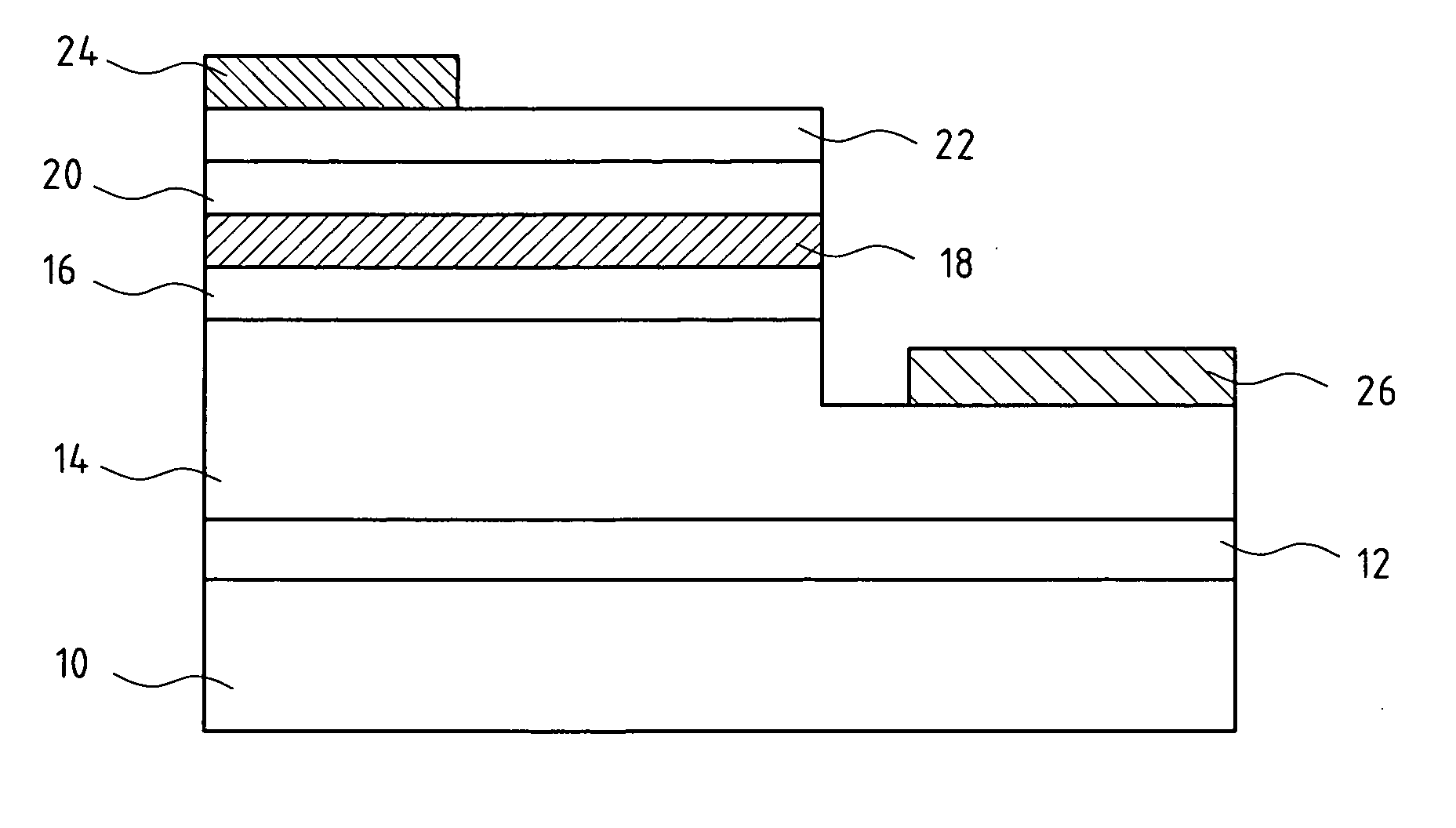
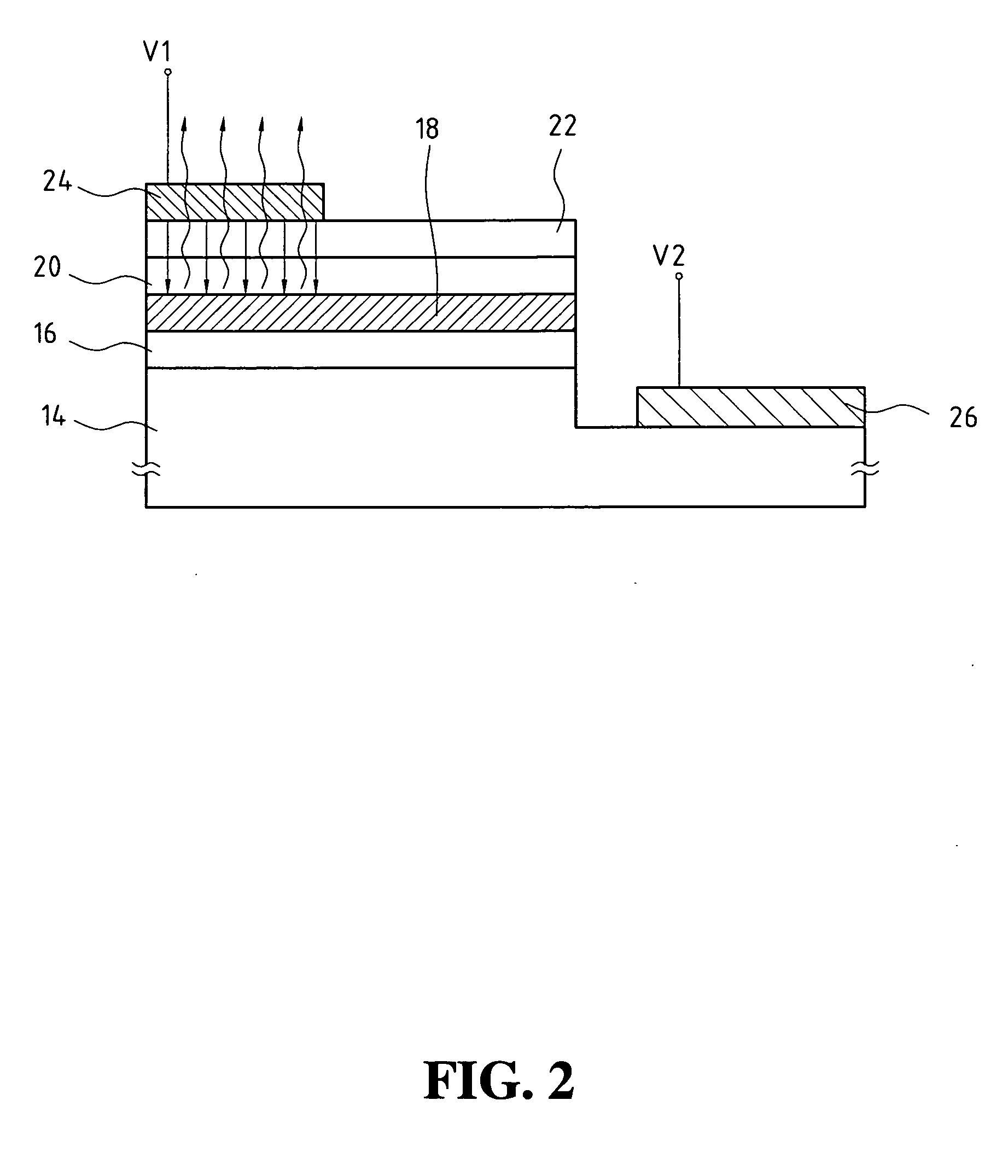
[0026] In a light emitting diode structure according to the present invention, a high carrier density (i.e. high conductivity) contact layer is formed using a Constructive Oxide Contact Structure contact layer to reduce the contact layer's resistance. When working with an appropriate transparent electrode, the contact layer can effectively increase a light emitting efficiency and reduce an operating voltage.

[0027] As the Constructive Oxide Contact Structure contact layer has a higher carrier density than that of a bulk layer, an Ohmic contact can be easily formed between the contact layer and the transparent electrode above. On the other hand, for a contact layer according to a prior art with a less carrier density, a Schottky contact could be formed and an ...


PUM


Abstract

Disclosed is a light emitting diode structure including a Constructive Oxide Contact Structure contact layer. The light emitting diode structure comprises a substrate, a buffer layer formed on the substrate, a lower confinement layer formed on the buffer layer, a light emitting layer formed on the lower confinement layer, an upper confinement layer formed on the light emitting layer, a Constructive Oxide Contact Structure contact layer formed on the upper confinement layer whose conducting type can be P-type, N-type, or I-type, a first electrode, and a second electrode (transparent electrode). The transparent electrode is formed on the Constructive Oxide Contact Structure contact layer as an anode of the light emitting diode. The first electrode is formed on the lower confinement layer and is spaced apart from the light emitting layer, the upper confinement layer, the contact layer, and the transparent electrode. The first electrode is used as a cathode of the light emitting diode.

Description

FIELD OF THE INVENTION [0001] The present invention relates to a light emitting diode structure, and more particularly, to a light emitting diode structure comprising III-V group elements and including a Constructive Oxide Contact Structure contact layer BACKGROUND OF THE INVENTION [0002] Gallium nitride (GaN) based blue light emitting diode has been industrialized on large scales worldwide since a group of Japanese researchers made a breakthrough in Gallium nitride (GaN) based extension technology in 1993. [0003] A conventional Gallium nitride (GaN) based light emitting diode structure, shown in FIG. 1, is constructed on a substrate 10 made of a material such as Al2O3. The light emitting diode 1 includes, sequentially from bottom to top, a nucleation layer 12, a N-type doped conducting buffer layer 14 made of N-type doped Gallium nitride (GaN) which makes a subsequent crystalline growth more smoothly and easily, a lower confinement layer 16, an active layer 18 for light emission, a...

Claims


Application Information

Patent Timeline
Patent Type & Authority Applications(United States)
IPC IPC(8): H01L29/22H01L33/02H01L33/14H01L33/32
CPCH01L33/02H01L33/14H01L33/32
Inventor HUANG, TING-KAILEE, CHI-SHENLAI, HUNG-CHANG
Owner HUGA OPTOTECH INC
Why Eureka
Try Eureka