Light emitting diode and method of making the same

a technology of light-emitting diodes and semiconductor chips, which is applied in the direction of liquid surface applicators, coatings, semiconductor devices, etc., can solve the problems of low efficiency, light is absorbed by the gaas substrate b>3, and conventional technologies still have some disadvantages and limitations, etc., to achieve high thermal conductivity coefficient, simple led structure, and improved light-emitting efficiency

Inactive Publication Date: 2006-03-16
EPISTAR CORP
View PDF8 Cites 10 Cited by
  • Summary
  • Abstract
  • Description
  • Claims
  • Application Information

AI Technical Summary

Benefits of technology

[0009] An advantage of the present invention is to provide a simple LED structure, wherein the adhesion process for forming the LED structure can be performed at a lower temperature to prevent the evaporation problem of V group elements. Moreover, because the light is not absorbed by the substrate, the light emitting efficiency of the LED can be significantly improved.
[0010] Another advantage of the present invention is the use of the elastic dielectric adhesive layer to bond the LED and the substrate having high thermal conductivity coefficient. Therefore, an excellent bonding result can be obtained by using the elastic dielectric adhesive layer even if the epitaxial structure has a rough surface.

Problems solved by technology

One disadvantage of the conventional LED is that, when the light generated by the active layer 5 is emitted downward to the GaAs substrate 3, the light is absorbed by the GaAs substrate 3 due to a smaller energy gap of the GaAs substrate 3.
However, these conventional technologies still have some disadvantages and limitations.
However, because the DBR layer only reflects the light almost normal to the GaAs substrate, its efficiency is not very great.
However, the fabrication process of TS AlGaInP LED is too complicated.
Therefore, it is difficult to manufacture these TS AlGaInP LEDs in high yield and low cost.

Method used


Image

  • Light emitting diode and method of making the same
  • Light emitting diode and method of making the same
  • Light emitting diode and method of making the same

Examples


Embodiment Construction

[0015] The present invention discloses a LED structure and a method of making the same, and will be described in details as follows.

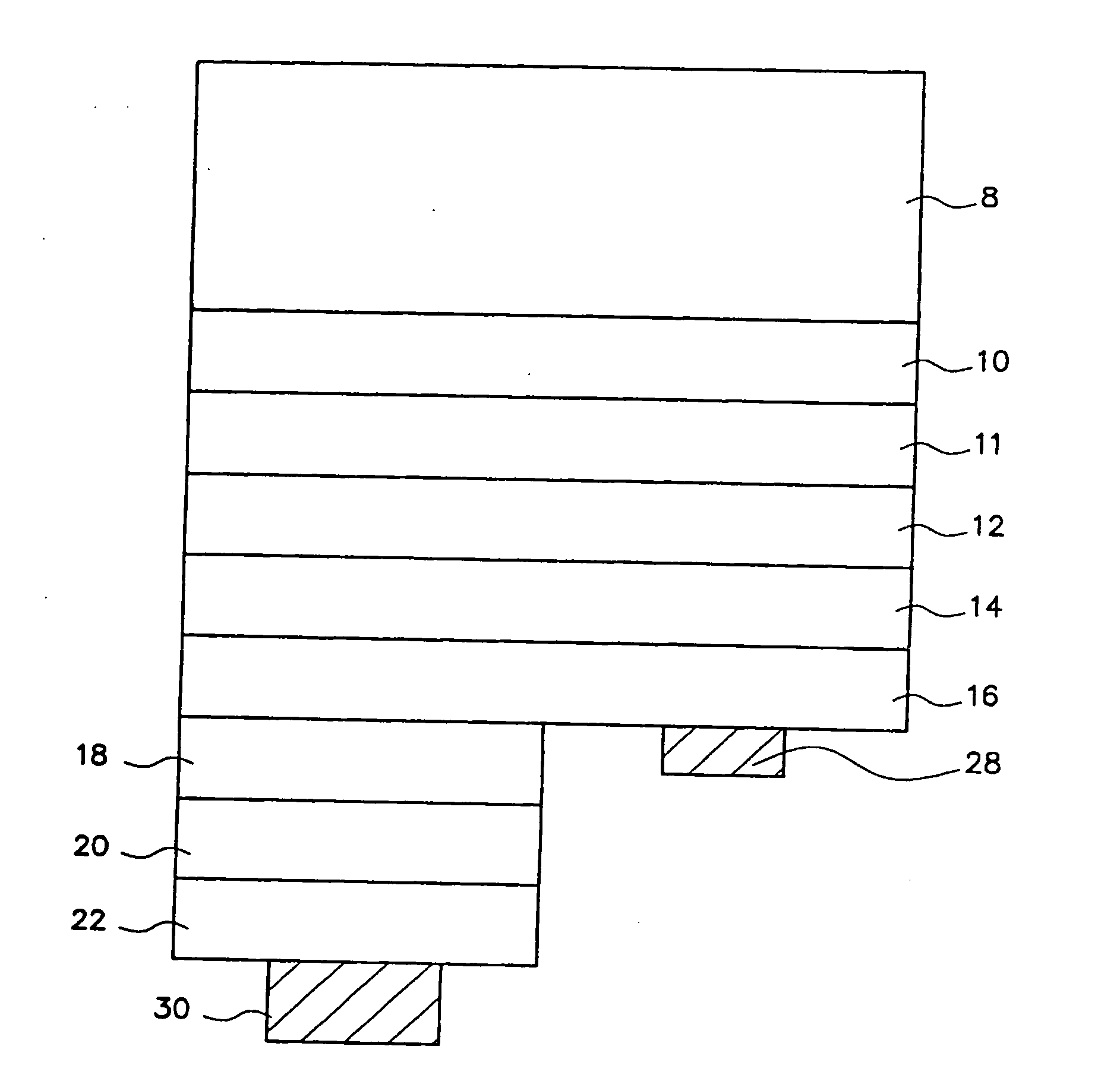
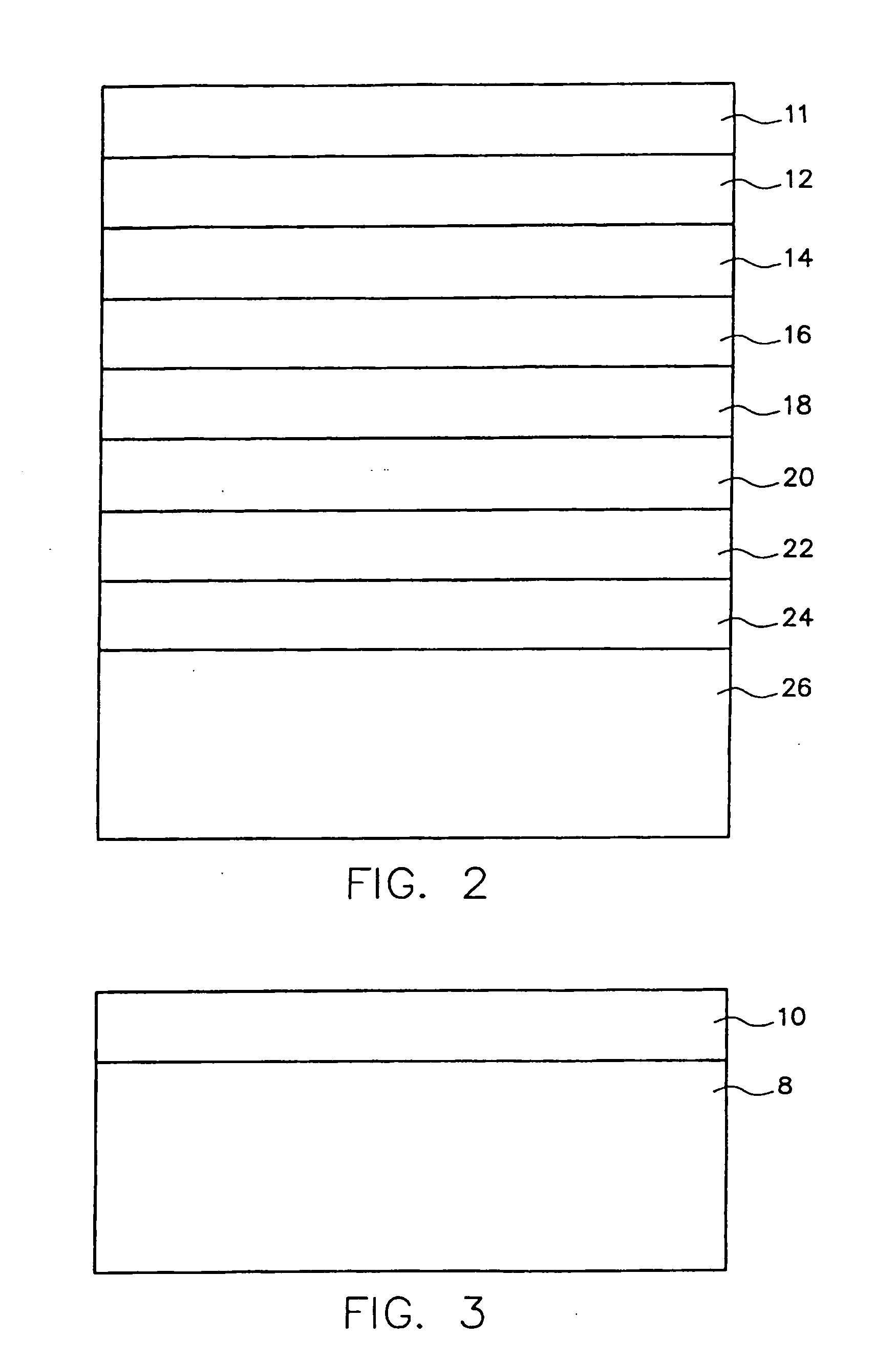
[0016] Referring to FIG. 2, the epitaxial structure of light emitting diode of the present invention is composed of an N-type GaAs substrate 26, an etching stop layer 24, an N-type (AlxGa1-x)0.5In0.5P lower cladding layer 22, an (AlxGa1-x)0.5In0.5P active layer 20, a P-type (AlxGa1-x)0.5In0.5P upper cladding layer 18, and a P-type ohmic contact epitaxial layer 16.

[0017] Thereafter, a mirror surface protection layer 14 is deposited over the P-type ohmic contact epitaxial layer 16, wherein the material of the mirror surface protection layer 14 is selected from a group consisting of SiNx, SiO2, Al2O3, magnesium oxide, zinc oxide, tin oxide, indium oxide, and indium tin oxide.

[0018] Thereafter, a metal mirror surface layer 12 is deposited over the mirror surface protection layer 14, wherein the material of the metal mirror surface layer 12 is selected fr...


PUM

PropertyMeasurementUnit
temperatureaaaaaaaaaa

Abstract

A light emitting diode (LED) and a method of making the same are disclosed. The present invention uses a metal layer of high conductivity and high reflectivity to prevent the substrate from absorbing the light emitted. This invention also uses the bonding technology of dielectric material thin film to replace the substrate of epitaxial growth with high thermal conductivity substrate to enhance the heat dissipation of the chip, thereby increasing the performance stability of the LED, and making the LED applicable under higher current.

Description

FIELD OF THE INVENTION [0001] The present invention relates to a structure and a method of making a light emitting diode (LED) chip, and more particularly to a structure and a method of making an AlGaInP LED chip. BACKGROUND OF THE INVENTION [0002] The conventional AlGaInP LED, as shown in FIG. 1, has a double heterostructure (DH), which is consisted of a N-type GaAs substrate 3 and a plurality of layers sequentially formed thereon, wherein the layers are: an N-type (AlxGa1-x)0.5In0.5P lower cladding layer 4 with an Al composition of about 70%˜100%, an (AlxGa1-x)0.5In0.5P active layer 5, a P-type (AlxGa1-x)0.5In0.5P upper cladding layer 6 with an Al composition of about 70%˜100% and a P-type high energy gap GaAsP, InGaP, AlGaP, GaP, or AlGaAs current spreading layer 7. The emitting wavelength of the conventional LED structure can be changed by adjusting the composition of the active layer 5 to a wavelength from 650 run red to 555 nm pure green. One disadvantage of the conventional L...

Claims


Application Information

Patent Timeline
Patent Type & Authority Applications(United States)
IPC IPC(8): H01L21/00H01L33/00H01L33/46H01L33/64
CPCH01L33/0079H01L2933/0075H01L33/64H01L33/46H01L33/0093
Inventor YANG, KUANG-NENG
Owner EPISTAR CORP
Why Eureka
Try Eureka