Very Small Pixel Pitch Focal Plane Array And Method For Manufacturng Thereof

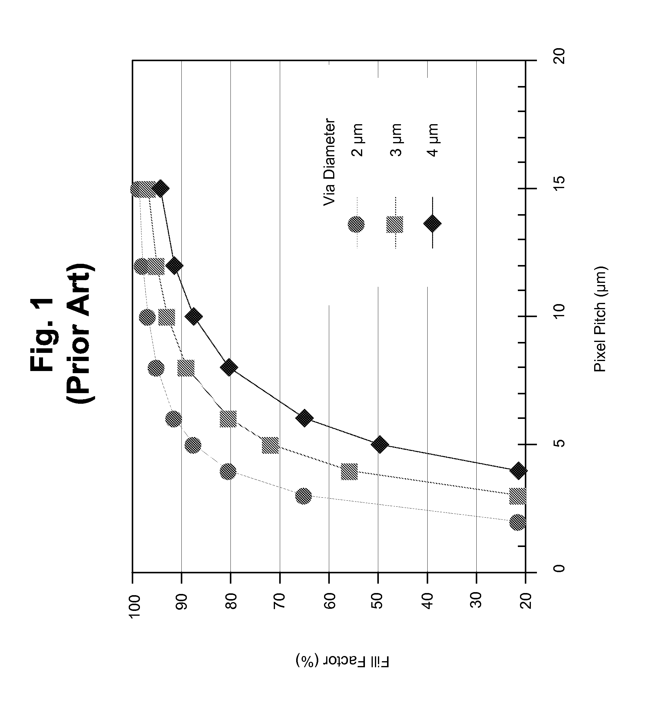
a focal plane array and very small pixel technology, applied in the field of imaging devices, can solve the problems of reducing the pixel pitch of conventional imaging devices or photodetectors, compromising the overall photodetector performance, and the image resolution that can be achieved from conventional infrared focal plane arrays (ir fpa), so as to achieve the effect of improving the focal plane architectur

Active Publication Date: 2010-04-01
DRS NETWORK & IMAGING SYST
View PDF11 Cites 14 Cited by
  • Summary
  • Abstract
  • Description
  • Claims
  • Application Information

AI Technical Summary

Benefits of technology

[0006]In accordance with systems and articles of manufacture consistent with the present invention, an imaging device having an improved focal plane architecture is provided. The imaging device comprises a semiconductor layer (such as an semiconductor infrared absorbing layer) and a photodetector having an implanted region formed in the semiconductor layer to define a p-n (or n-p) junction therein, and a pad formed or deposited over the implanted region. The pad has a malleable metal or metallic material, such as Indium. The imaging device further comprises a readout circuit having a contact plug. The contact plug has a base and a prong extending from the base and into the malleable metallic material of the pad. In one implementation, the prong is a first of a plurality of prongs extending from the base and into the malleable metallic material of the pad. The prongs have a structure effective to displace a portion of the malleable metallic material into a space between the first prong and a second of the prongs.

Problems solved by technology

The image resolution that can be achieved from conventional infrared focal plane arrays (IR FPA), even with the most favorable optics, are generally limited by the pixel pitch.
Among the primary limitations in reducing the pixel pitch of conventional imaging devices or photodetectors are the architecture of the FPA and associated readout circuit contacts and the fabrication technique for electrical interconnection of the FPA to the unit cells of the associated readout circuit.
As shown in FIG. 1, for smaller pixel pitches (e.g., less than 6 microns), the fill factor drops rapidly even for a via diameter of 2 microns and, thus, compromises the overall photodetector performance.

Method used


Image

  • Very Small Pixel Pitch Focal Plane Array And Method For Manufacturng Thereof
  • Very Small Pixel Pitch Focal Plane Array And Method For Manufacturng Thereof
  • Very Small Pixel Pitch Focal Plane Array And Method For Manufacturng Thereof

Examples


Embodiment Construction

[0017]Reference will now be made in detail to an implementation in accordance with methods, systems, and products consistent with the present invention as illustrated in the accompanying drawings.

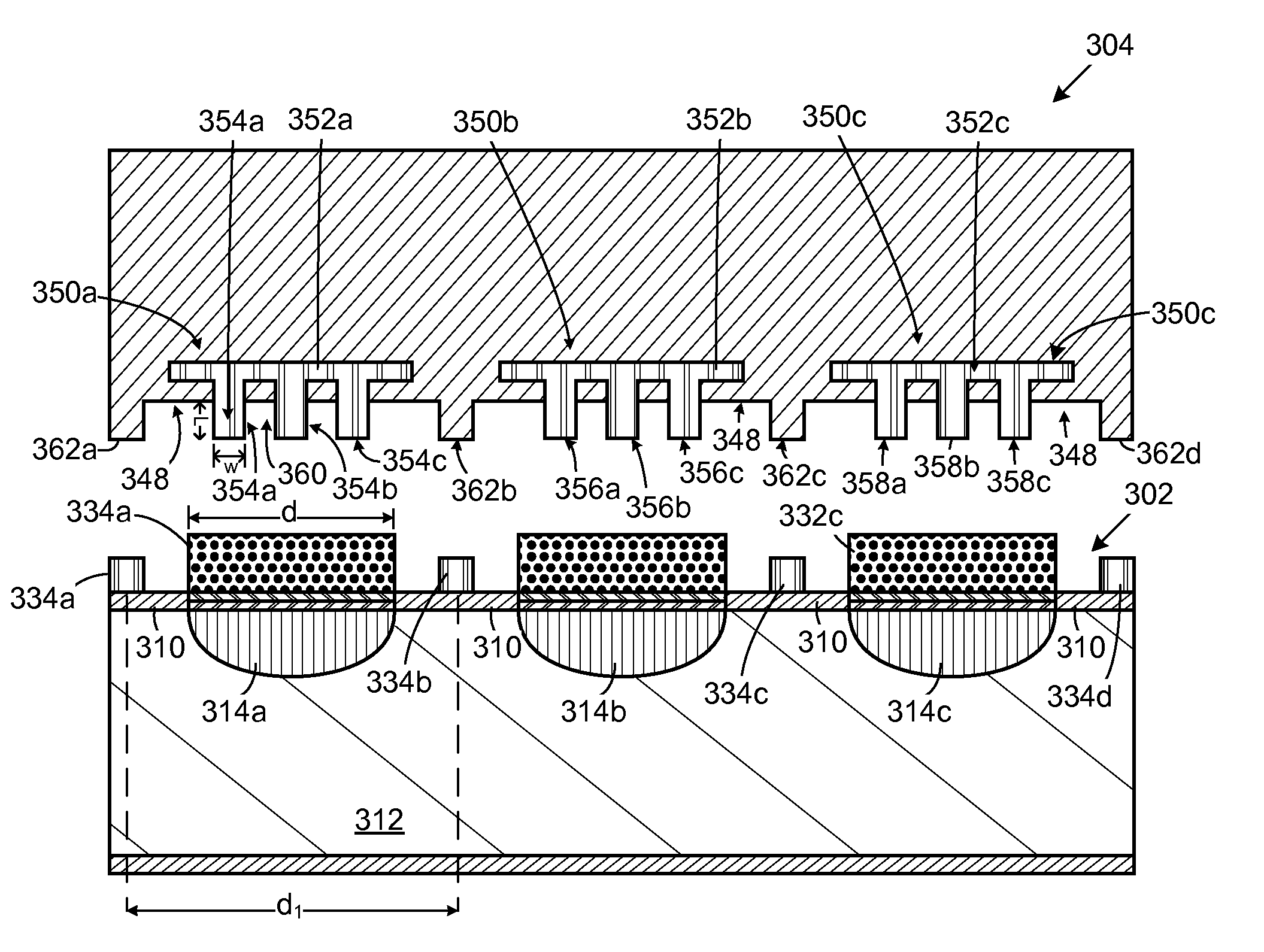
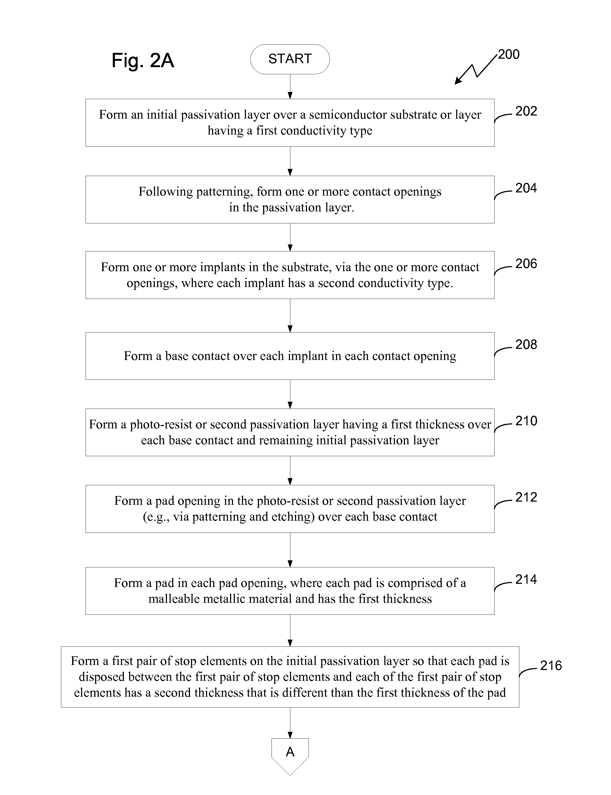
[0018]Methods consistent with the present invention provide a process 200 depicted in FIGS. 2A-2B for manufacturing a focal plane array (FPA) of an imaging device, where an array of photodetectors with dimensions comparable to the cutoff wavelength of the respective photodetector is aligned with and interconnected to a unit cell of a readout integrated circuit (ROIC or readout circuit) to enable the realization of very small pixel pitches. FIGS. 3A to 3F and 3H to 3J are cross sectional views of an exemplary photodetector array 302 and an exemplary ROIC 304 of an imaging device 300 (as completed in FIG. 3J), where the photodetector array 302 and the ROIC 304 are illustrated at various steps of the manufacturing process 200. FIG. 3G is a top level view of the exemplary photodetector array 30...


PUM


Abstract

A method for manufacturing an imaging device is provided. The method comprises forming a contact pad over a semiconductor substrate. The contact pad has a malleable metal. The method further comprises providing a readout circuit having a first side and a contact plug. The contact plug has a base affixed to the first side of the readout circuit and a plurality of prongs extending from the base away from the first side. The first side of the readout circuit is moved towards the substrate so that the prongs of the contact plug are pressed into the pad and displace a portion of the pad into a space defined by and between a first and a second of the prongs. Stop elements formed over the substrate are aligned with and contact stop elements provided on the readout circuit so that the prongs are inhibited from passing completely through the contact pad.

Description

FIELD OF THE INVENTION[0001]The present invention relates to imaging devices. More particularly, the present invention relates to an imaging device having a focal plane array with a readout circuit and method of manufacturing thereof, where each pixel of the focal plane array has a very small pitch with dimensions corresponding to the cutoff wavelength of the photodetector of the respective pixel.BACKGROUND OF THE INVENTION[0002]The image resolution that can be achieved from conventional infrared focal plane arrays (IR FPA), even with the most favorable optics, are generally limited by the pixel pitch. In the most advanced conventional FPAs, the smallest pixel pitch dimensions are 12 microns for mid wavelength (MW) IR with a nominal cutoff wavelength of 5 microns. In the long wavelength (LW) IR bands with cutoff wavelengths of around 10 microns, the smallest pixel pitch observed by the applicant for conventional FPAs is 15 microns.[0003]To enhance and further optimize image resoluti...

Claims


Application Information

Patent Timeline
Patent Type & Authority Applications(United States)
IPC IPC(8): H04N5/335
CPCH01L27/14618H01L27/14634H01L27/14636H01L27/1469H01L27/1464H04N5/3696H01L2224/81193H01L2224/81141H01L27/14696H01L27/14687H01L27/14647H01L27/14694H01L27/14645
Inventor MITRA, PRADIP
Owner DRS NETWORK & IMAGING SYST
Why Eureka
Try Eureka