Multilayer circuit board and method for manufacturing the same

a multi-layer circuit board and manufacturing method technology, applied in the direction of resistive material coating, lithographic masks, metal masks, etc., can solve the problem of measurable deformation of the hard core layer, and achieve the effect of reducing the thickness of the second resin layer, reducing the thickness of the core layer, and eliminating desmear treatmen

Active Publication Date: 2010-04-08
TDK CORPARATION
View PDF14 Cites 10 Cited by
  • Summary
  • Abstract
  • Description
  • Claims
  • Application Information

AI Technical Summary

Benefits of technology

[0006]The present invention is proposed to resolve these problems. Therefore, an object of the present invention is to provide a multilayer circuit board assuring reliable products and allowing the entire circuit board to have a smaller thickness and a method for manufacturing the same.
[0007]Another object of the present invention is to provide a semiconductor IC-embedded multilayer circuit board assuring reliable products and allowing the entire circuit board to have a smaller thickness and a method for manufacturing the same.

Problems solved by technology

However, even this hard core layer is subject to measurable deformation when it has a thickness reduced to 100 μm or smaller.

Method used


Image

  • Multilayer circuit board and method for manufacturing the same
  • Multilayer circuit board and method for manufacturing the same
  • Multilayer circuit board and method for manufacturing the same

Examples


Embodiment Construction

[0083]Preferred embodiments of the present invention will now be explained in detail with reference to the drawings.

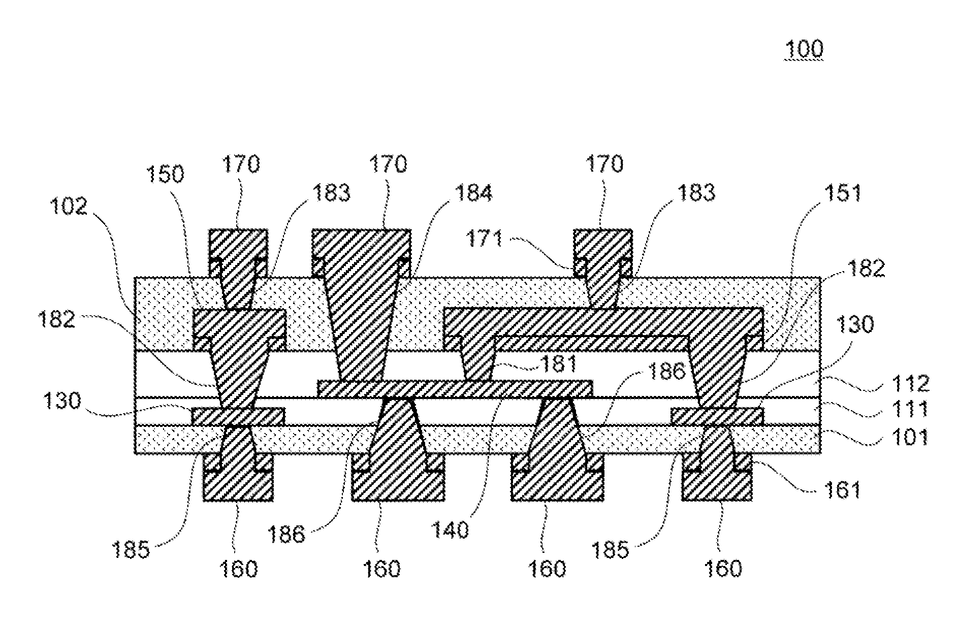
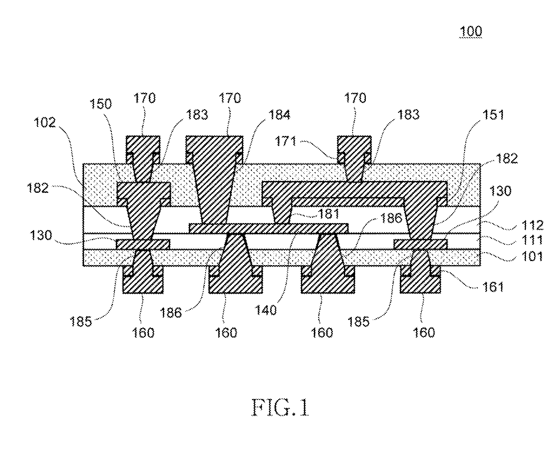
[0084]FIG. 1 is a schematic sectional view showing the structure of a multilayer circuit board 100 according to a first preferred embodiment of the present invention.

[0085]As shown in FIG. 1, the multilayer circuit board 100 of this embodiment includes outermost core layers 101 and 102, resin layers 111 and 112 positioned between the core layers 101 and 102, wiring patterns 130, 140, 150, 160, and 170, and through electrodes 181 to 186. Among them, the wiring pattern 130 is embedded between the core layer 101 and the resin layer 111; the wiring pattern 140 is embedded between the resin layers 111 and 112; and the wiring pattern 150 is embedded between the resin layer 112 and the core layer 102. The wiring pattern 160 is formed on the surface of the core layer 101 and the wiring pattern 170 is formed on the surface of the core layer 102. Passive components such as capac...


PUM

PropertyMeasurementUnit
thicknessaaaaaaaaaa
thicknessaaaaaaaaaa
thicknessaaaaaaaaaa

Abstract

A multilayer circuit board comprises core layers 101 and 102 made of a core material impregnated with resin, resin layers 111 and 112 interposed between the core layers 101 and 102, a wiring pattern 140 embedded in the resin layers 111 and 112. The core layers 101 and 102 have a thickness of 100 μm or smaller, whereby the entire board can significantly be thinned. Furthermore, the less strong resin layers 111 and 112 are interposed between the hard core layers 101 and 102, whereby the entire board has increased strength.

Description

TECHNICAL FIELD[0001]The present invention relates to a multilayer circuit board and a method for manufacturing the same, and particularly to a multilayer circuit board assuring reliable products and allowing the entire circuit board to have a smaller thickness and a method for manufacturing the same.BACKGROUND OF THE INVENTION[0002]A multilayer circuit board in which wiring patterns and semiconductor ICs are embedded usually has a thick core layer made of a core material such as a glass cloth impregnated with resin to prevent the board from being distorted or deformed in the course of production.[0003]However, the core layer tends to increase the thickness of the multilayer circuit board. Therefore, demand for thinned is not fulfilled in some cases. A method to reduce the thickness of the entire board is to form a board using only thin resin layers and no core layer. In this way, the board is subject to significant distortion in the course of production. This distortion causes no p...

Claims


Application Information

Patent Timeline
Patent Type & Authority Applications(United States)
IPC IPC(8): H05K3/30H05K3/10
CPCH01L23/49822Y10T428/24917H01L24/24H01L24/82H01L2224/24226H01L2224/82039H01L2224/82047H01L2224/92H01L2224/92244H01L2924/01015H01L2924/01029H01L2924/0103H01L2924/01033H01L2924/01061H01L2924/01078H01L2924/01079H01L2924/14H01L2924/19041H05K1/185H05K3/0044H05K3/0058H05K3/4602H05K3/4652H05K3/4682H05K3/4688H05K2201/0358H05K2201/09518H05K2201/09527H05K2201/09563H05K2203/0152H05K2203/025H05K2203/0554H05K2203/1105H05K2203/1476H05K2203/1572H01L23/5389Y10T29/49128H01L2224/2518H01L2924/01005H01L2924/01006H01L2924/01024H01L2924/01047H01L2924/014H01L2224/83H01L2224/82H01L2924/12042H01L2924/00
Inventor KAWABATA, KENICHIMORITA, TAKAAKI
Owner TDK CORPARATION
Why Eureka
Try Eureka