

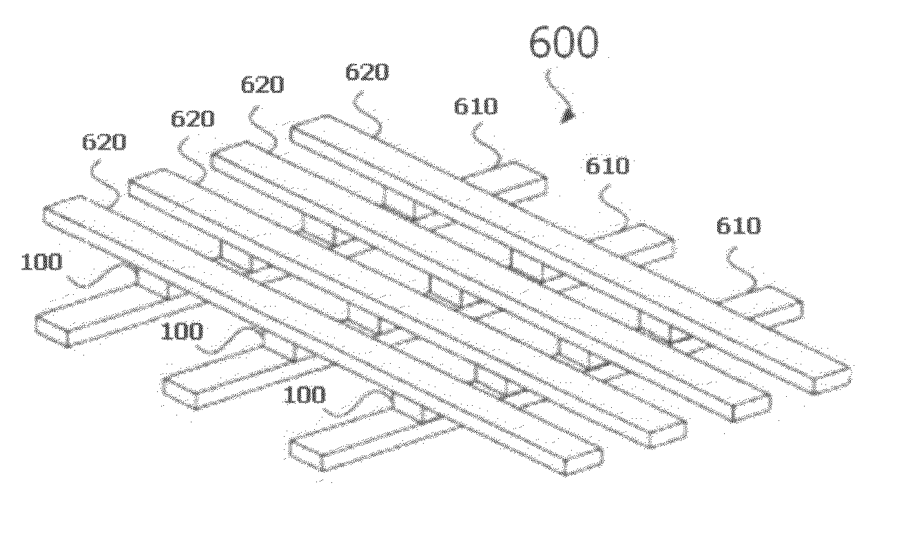
Nanoscale electrical device
a technology of electrical devices and nano-scales, applied in the direction of semiconductor devices, bulk negative resistance effect devices, electrical apparatus, etc., can solve the problems of multiple physical barriers, increase ic cost, and high cost of silicon real estate, and achieve high impedance states
- Summary
- Abstract
- Description
- Claims
- Application Information
AI Technical Summary
Benefits of technology
Problems solved by technology
Method used
Image

Examples
Embodiment Construction
[0040]Tentative explanations are given for some of the observed phenomena in invented device. Such theoretical considerations are not to be construed as limiting the appended claims that are set forth in terms of measurable device parameters. Postulated mechanisms set forth in this section as well as that preceding are intended to aid the practitioner to make specific utilization of device characteristics.
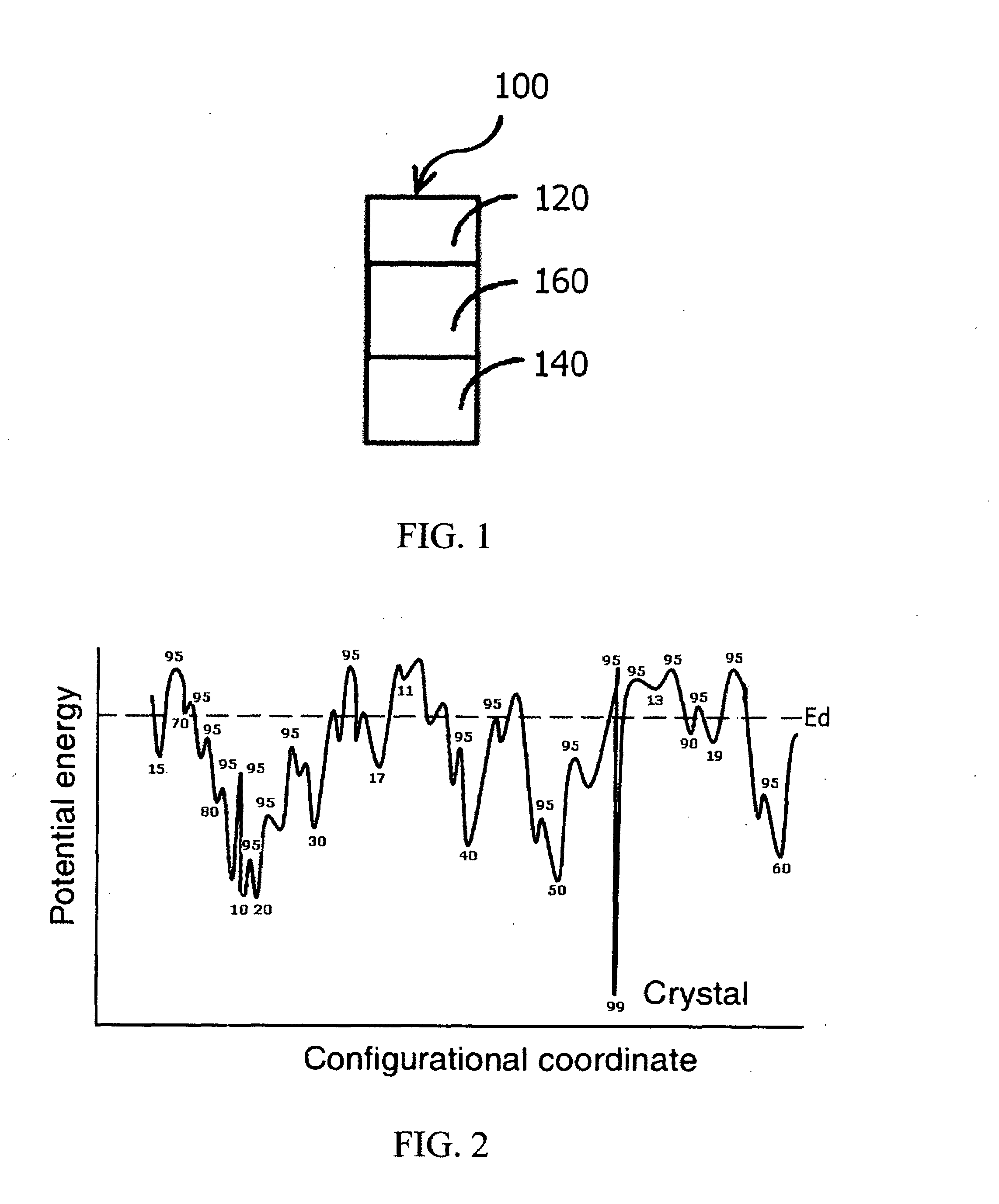
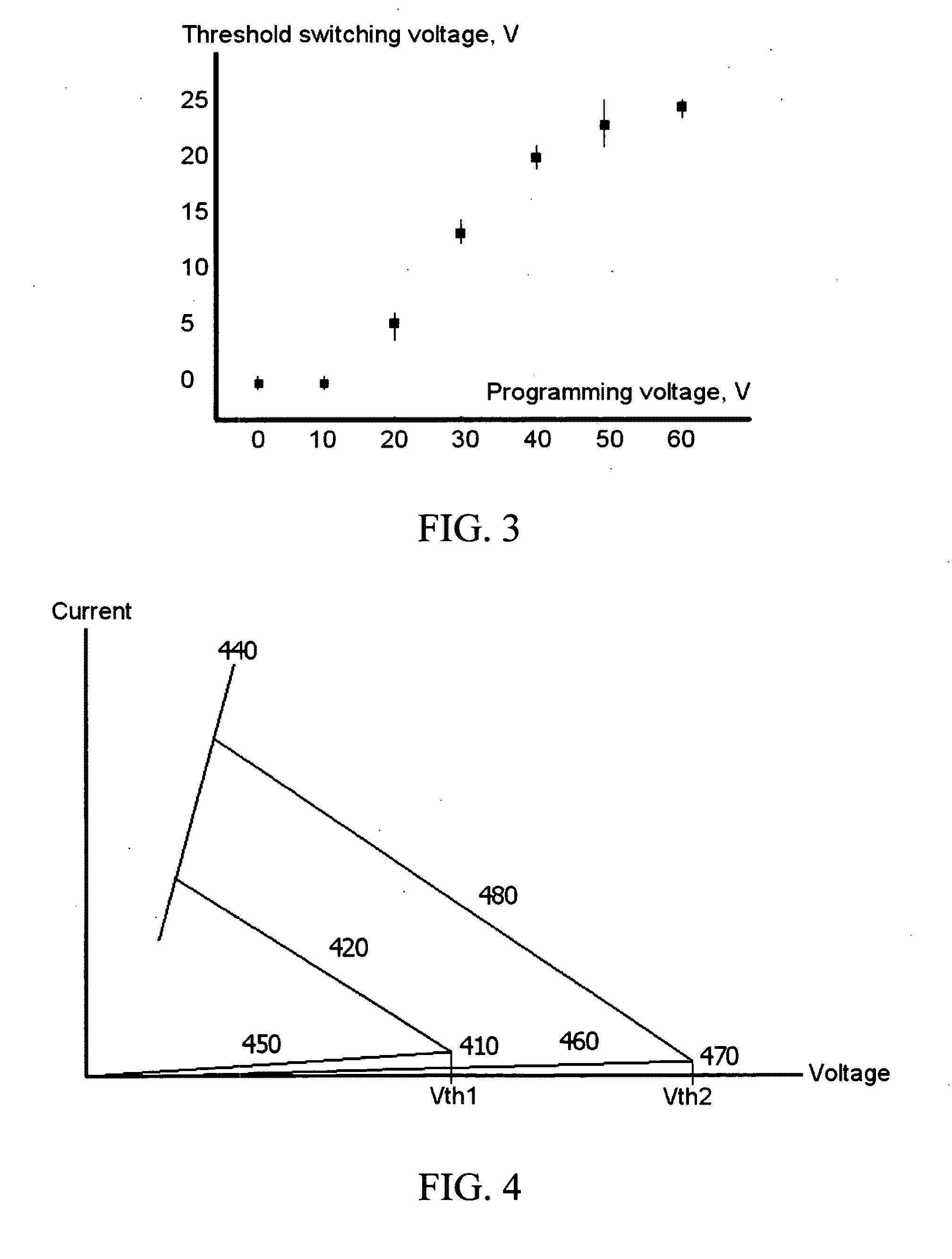
[0041]The description in terms of the experimental results obtained with invented device shown in FIG. 1 which yielded the data plotted in FIG. 3 and FIG. 5.
[0042]FIG. 1 shows the invented device 100 that compromises a disordered material 160 between a first electrode 120 and a second electrode 140. The methods of manufacturing of the invented device 100 consist of deposition and pattering of the first electrode 140, then deposition and pattering of the disordered material 160 and finally deposition and pattering of the second electrode 120. In some embodiments CVD or / and PVD are u...
PUM
 Abstract
Description
Claims
Application Information