
Active pixel senor circuit

a technology of active pixel and sensor circuit, which is applied in the field of active pixel sensor, can solve the problems of increasing the amount of charges generated and increasing the consumption of display power

Active Publication Date: 2010-04-15
AU OPTRONICS CORP
View PDF7 Cites 24 Cited by
  • Summary
  • Abstract
  • Description
  • Claims
  • Application Information

AI Technical Summary

Benefits of technology

[0002]Generally, CMOS active pixel sensors utilize amplifiers built in each pixel to amplify photovoltaic signals generated by photosensors in response to illumination of light, which can be readout selectively according to an X-Y address of each pixel. For such CMOS active pixel sensors, the photovoltaic signals are amplified by the built-in amplifiers before being transmitted to external control circuits, thereby eliminating noises associated with transmitting passes of the signals.

Problems solved by technology

An increase in the area leads to an increase in the amount of charges generated.
For a fixed amount of brightness of the display, the brightness of the backlight illuminating the display must be increased, thereby increasing the consumption of power of the display.

Method used


Image

  • Active pixel senor circuit
  • Active pixel senor circuit
  • Active pixel senor circuit

Examples


Embodiment Construction

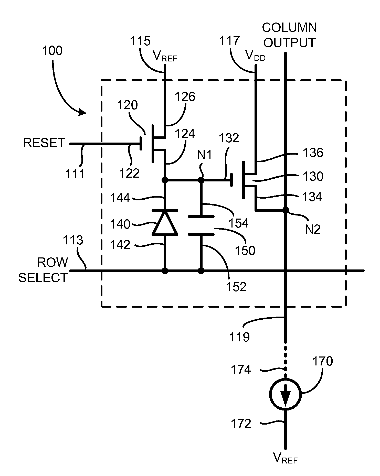
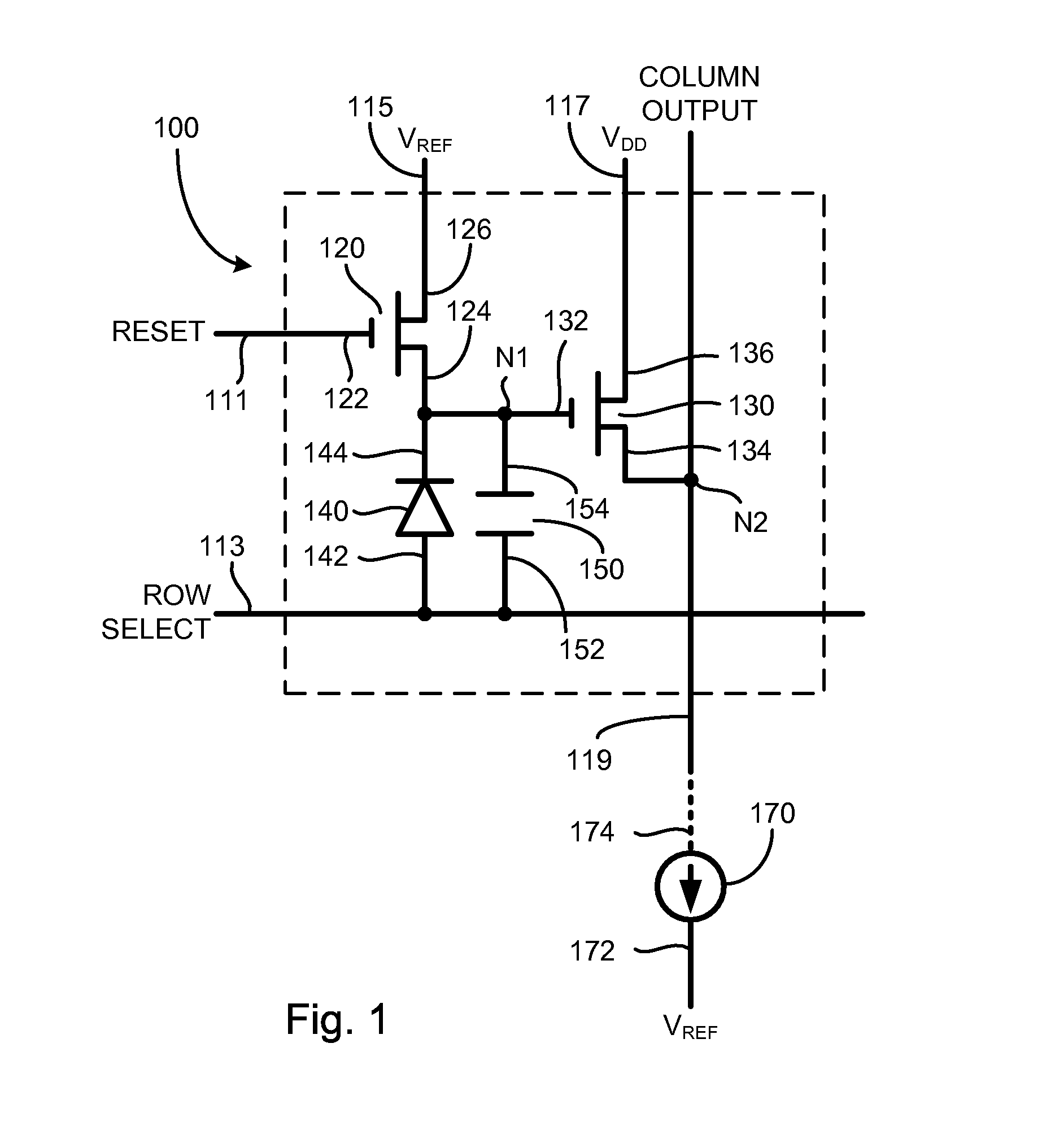
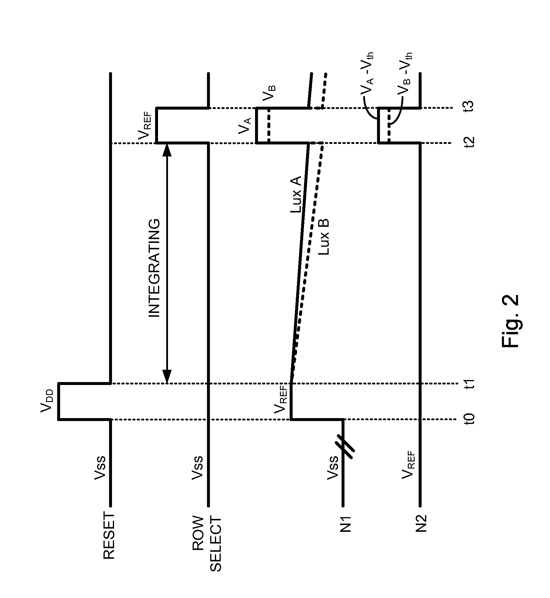
[0039]The present invention is more particularly described in the following examples that are intended as illustrative only since numerous modifications and variations therein will be apparent to those skilled in the art. Various embodiments of the invention are now described in detail. Referring to the drawings, like numbers indicate like components throughout the views. As used in the description herein and throughout the claims that follow, the meaning of “a”, “an”, and “the” includes plural reference unless the context clearly dictates otherwise. Also, as used in the description herein and throughout the claims that follow, the meaning of “in” includes “in” and “on” unless the context clearly dictates otherwise.

[0040]The terms used in this specification generally have their ordinary meanings in the art, within the context of the invention, and in the specific context where each term is used. Certain terms that are used to describe the invention are discussed below, or elsewhere ...


PUM


Abstract

The present invention relates to an active pixel sensor circuit and a method of operating same. In one embodiment, the active pixel sensor circuit includes a reset transistor having a gate, a source and a drain, a silicon rich oxide (SRO) photosensor having an anode and a cathode electrically coupled to the source of the reset transistor, and a readout transistor having a gate electrically coupled to the cathode of the SRO photosensor, a source and a drain.

Description

FIELD OF THE INVENTION[0001]The present invention relates to an active pixel sensor, and more particularly to an active pixel sensor circuit that utilizes a two-transistor design to improve aperture ratio and sensitivity.BACKGROUND OF THE INVENTION[0002]Generally, CMOS active pixel sensors utilize amplifiers built in each pixel to amplify photovoltaic signals generated by photosensors in response to illumination of light, which can be readout selectively according to an X-Y address of each pixel. For such CMOS active pixel sensors, the photovoltaic signals are amplified by the built-in amplifiers before being transmitted to external control circuits, thereby eliminating noises associated with transmitting passes of the signals.[0003]It is known that the sensitivity of an active pixel sensor is determined by at least three factors. The first factor is related to the area in the active pixel sensor available for converting photons to electrons. An increase in the area leads to an incr...

Claims


Application Information

Patent Timeline
IPC IPC(8): H04N5/335
CPCH04N5/374H04N25/76
Inventor CHUANG, MING-HUNGCHO, AN-THUNG
Owner AU OPTRONICS CORP
Learn More