Coordinate input device and display device with the same

a display device and input signal technology, applied in the field of coordinate input devices, can solve the problems of reducing the dynamic range of the input signal after the ad conversion, the change of the charging period of time required, and the reduction of the measuring accuracy, so as to improve the detection accuracy, the dynamic range of the detectable input capacitance is widened, and the input capacitance to be increased.

Active Publication Date: 2010-04-08
PANASONIC LIQUID CRYSTAL DISPLAY CO LTD +1
View PDF12 Cites 140 Cited by
  • Summary
  • Abstract
  • Description
  • Claims
  • Application Information

AI Technical Summary

Benefits of technology

[0019]According to the present invention, only the input capacitance to be increased by touching may be detected as the output signal. Thus, a dynamic range of the detectable input capacitance is widened, and

Problems solved by technology

As a result, a charging potential of the electric charge storage capacitor charged to a fixed potential beforehand is lowered, causing a change in charging period of time required until the electric charge storage capacitor is charged to the fixed potential again.
However, when the sensor employing the capacitance detection method disclosed in U.S. Pat. No. 6,466,036 or U.S. Pat. No. 7,312,616 is installed close to a display surface of a display device such as a liquid crystal display, influence o

Method used


Image

  • Coordinate input device and display device with the same
  • Coordinate input device and display device with the same
  • Coordinate input device and display device with the same

Examples


first embodiment

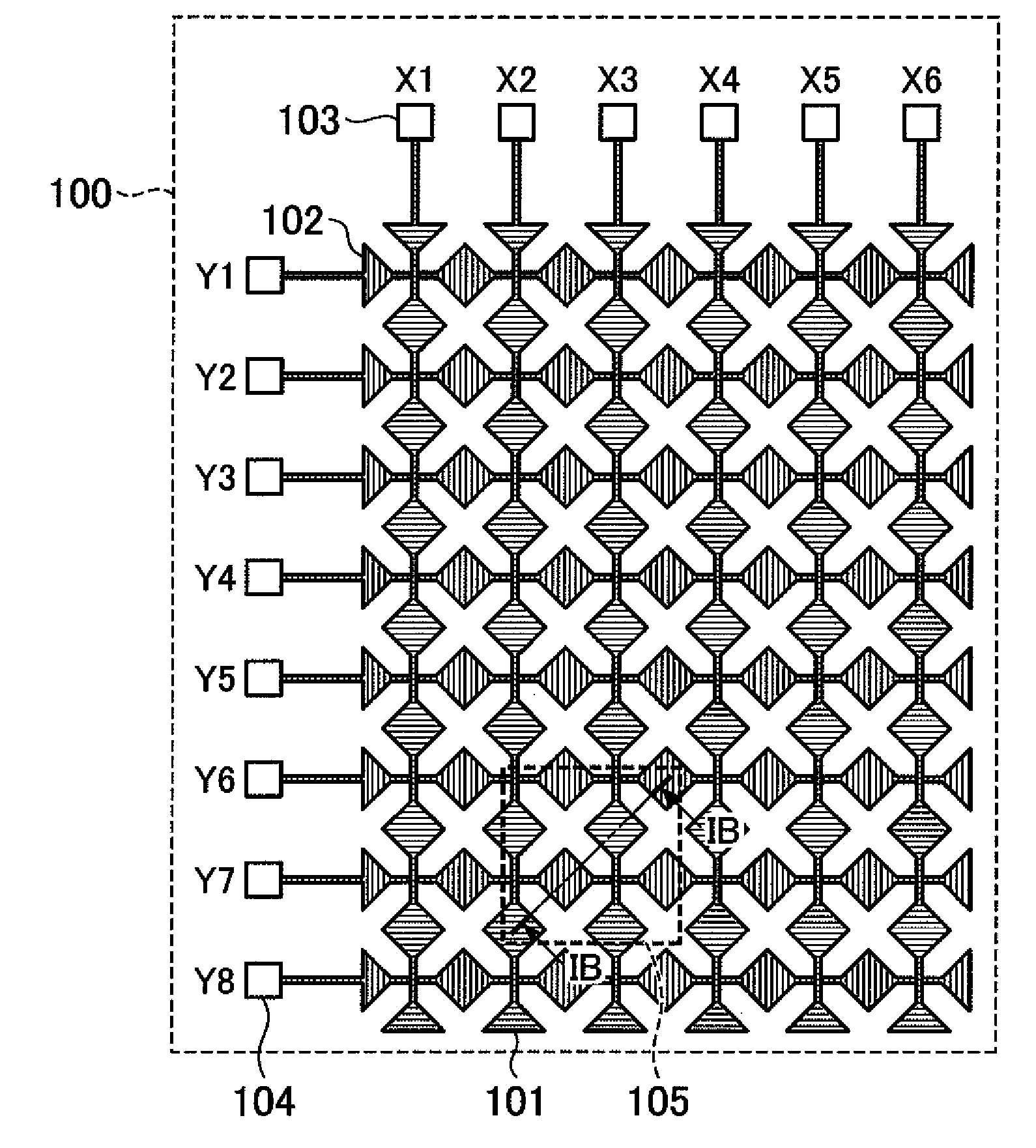
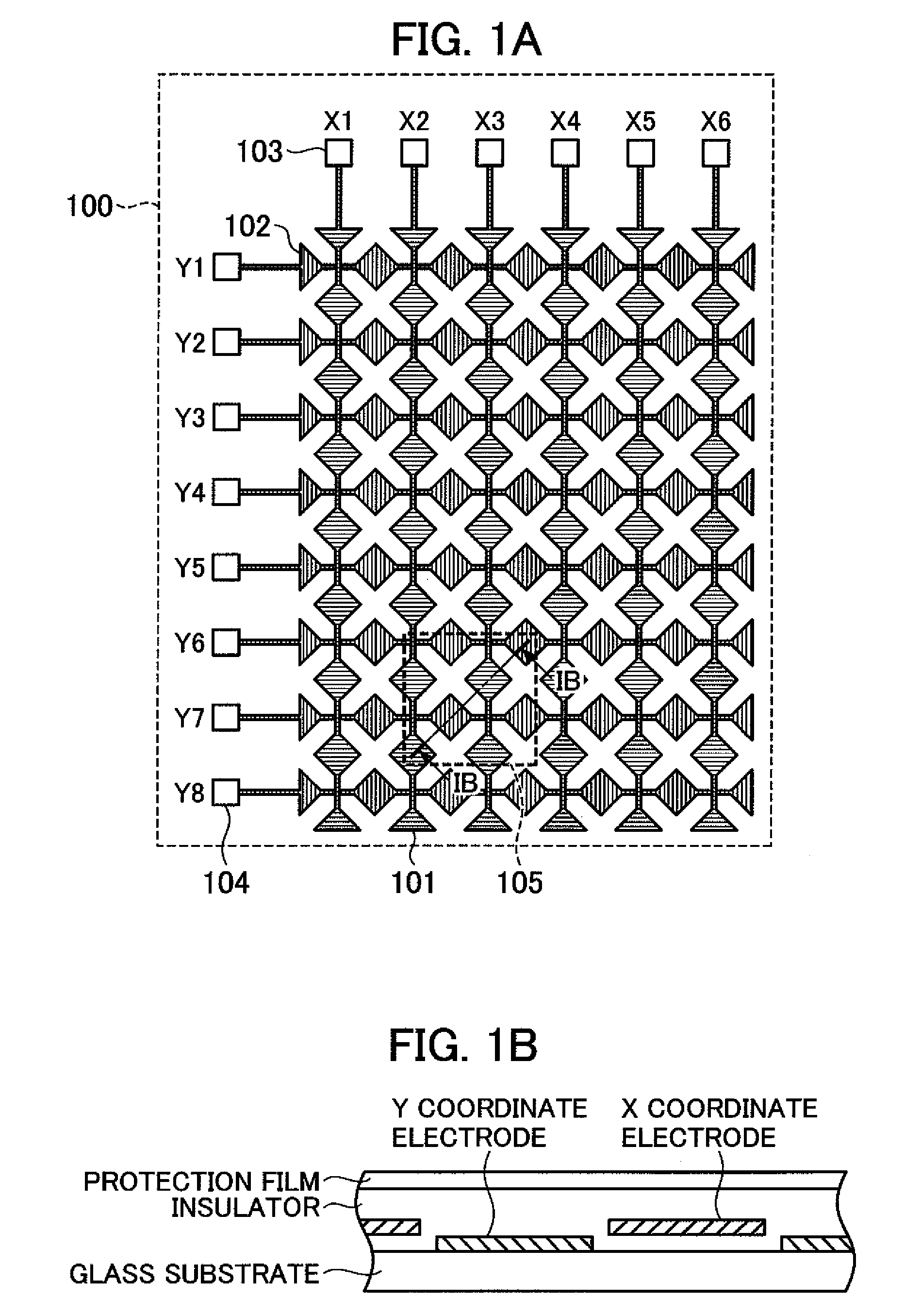
[0067]FIGS. 1A and 1B are schematic diagrams each illustrating a configuration example of a touch sensor panel according to a first embodiment of the present invention. FIG. 1A illustrates a planar configuration of a touch sensor panel 100. In order to detect touching by a finger or the like, a plurality of X coordinate electrodes 101 and a plurality of Y coordinate electrodes 102 are disposed. The X coordinate electrodes are connected in a column direction. The Y coordinate electrodes are connected in a row direction. Electrode terminals 103 and 104 are disposed for each group of such connected electrodes to enable electrical signal extraction.

[0068]FIG. 1B illustrates a sectional structure of the touch sensor panel 100. FIG. 1B is a cross sectional diagram along an IB-IB cutting line of an area 105 illustrated in FIG. 1A. There is an insulating layer on a substrate made of a material such as glass. In the insulating layer, each of the X coordinate electrodes and each of the Y coor...

second embodiment

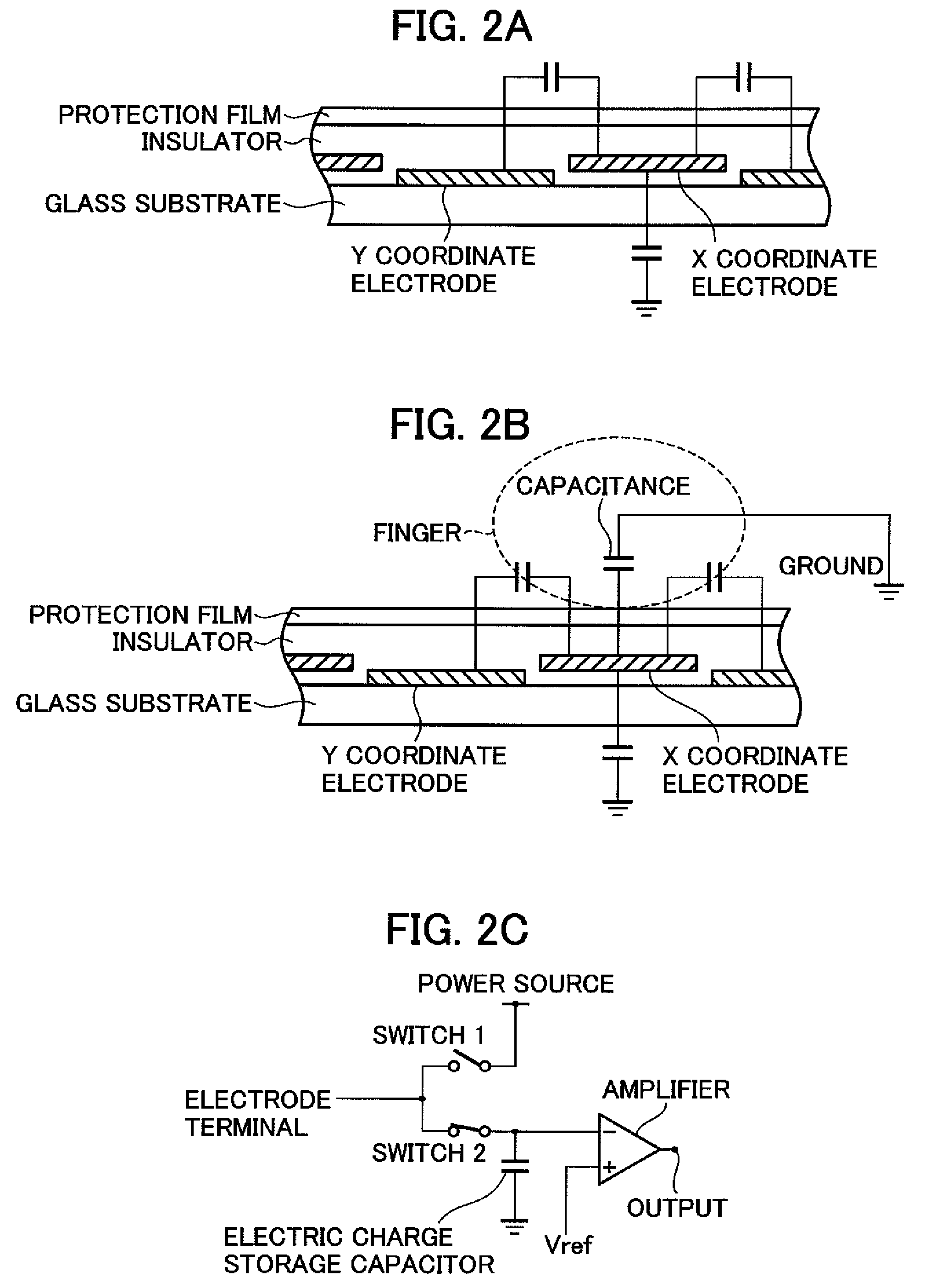
[0078]FIGS. 11A and 11B illustrate a second embodiment of the present invention. In this embodiment, as illustrated in FIG. 11A, a switch 5 and a switch 6 are added to the configuration of the first embodiment. One end of each of the switches 5 and 6 is connected to a reference potential of a voltage source for generating a reference potential Vref of an amplifier. The other end of the switch 5 is connected to a reference potential side of an electric charge storage capacitor, and the other end of the switch 6 is connected to a ground. Operations of switches 3 and 4 are similar to those of the first embodiment. The switch 5 and the switch 6 respectively operate in synchronization with the switch 3 and the switch 4. FIG. 11B illustrates effects of this embodiment. The switch 5 operates in synchronization with the switch 3 to set the reference potential of the voltage source for generating the reference potential Vref of the amplifier as a potential of a transparent electrode 1. Poten...

third embodiment

[0079]Hereinafter, an embodiment in which the present invention is applied to a detection system for a capacitance based on a successive approximate capacitance system is described.

[0080]FIGS. 12A and 12B are conceptual diagrams illustrating capacitance measurement by the successive approximate capacitance system. FIG. 12A illustrates a state where a capacitance is connected to the detection circuit of the successive approximate capacitance system. FIG. 12B illustrates an operation of the successive approximate capacitance system. A switch 1 and a switch 2 in the circuit illustrated in FIG. 12A are alternately turned ON and OFF repeatedly for a given period of time. When the switch 1 is turned ON (switch 2 is OFF), a detected capacitance illustrated in FIG. 12A is charged. In this case, the charged electric charges are supplied from a constant current source and an electric charge storage capacitor. Then, when the switch 2 is turned ON (switch 1 is OFF), electric charges charged in ...


PUM


Abstract

A capacitance detection device of a capacitance system includes: a capacitance sensor electrode for detecting a capacitance; a power source for supplying charges to be charged in the capacitance sensor electrode; an electric charge storage capacitor in which an amount of charges to be charged therein changes according to the electric charges charged in the capacitance sensor electrode; and a switch for changing a reference potential of the electric charge storage capacitor. The reference potential of the electric charge storage capacitor is changed in a period of measuring the capacitance.

Description

CROSS-REFERENCE TO RELATED APPLICATIONS[0001]The present application claims priority from Japanese applications JP2008-259588 filed on Oct. 6, 2008 and JP2009-098659 filed on Apr. 15, 2009, the contents of which are hereby incorporated by reference into this application.BACKGROUND OF THE INVENTION[0002]1. Field of the Invention[0003]The present invention relates to a coordinate input device for inputting coordinates to a screen, and a display device including the same, and more particularly, to a technology suitable for achieving high coordinate detection accuracy in a coordinate input device of a capacitive coupling system.[0004]2. Description of the Related Art[0005]An image display device that has a sensor function in a display screen and a screen input function of inputting information by a touching operation using a finger or a stylus pen is used for a mobile electronic device such as a PDA or a portable terminal, various home electric appliances, or a stationary customer guida...

Claims


Application Information

Patent Timeline
IPC IPC(8): G06F3/041G01R27/26
CPCG06F3/044G06F3/0418G06F3/0446G06F1/3262G06F3/0412
Inventor MAMBA, NORIONAGATA, KOJIHAYAKAWA, KOJIANNO, KOUICHIKUMAGAI, TOSHIYUKIFURUHASHI, TSUTOMUKAJIWARA, HISAYOSHI
Owner PANASONIC LIQUID CRYSTAL DISPLAY CO LTD
Why Eureka
Try Eureka