

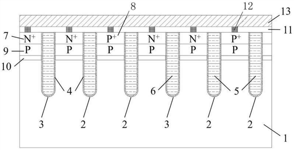
IGBT trench gate arrangement structure
A trench gate, trench gate technology, applied in electrical components, circuits, semiconductor devices, etc., can solve the problems of small input capacitance and Miller capacitance, uneven channel current distribution, small current gate oscillation, etc. Input capacitance and Miller capacitance, uniform current distribution, and the effect of increasing the setting ratio
- Summary
- Abstract
- Description
- Claims
- Application Information
AI Technical Summary
Problems solved by technology
Method used
Image

Examples
Embodiment Construction
[0012] The present invention will be further described below in conjunction with the accompanying drawings. The following examples are only used to illustrate the technical solution of the present invention more clearly, but not to limit the protection scope of the present invention.
[0013] It should be noted that, in the description of the present invention, the terms "front", "rear", "left", "right", "upper", "lower", "inner", "outer" and the like indicate orientations or positions The relationship is based on the orientation or positional relationship shown in the drawings, and is only for the convenience of describing the present invention and does not require that the present invention must be constructed and operated in a specific orientation, and thus should not be construed as a limitation of the present invention. The terms "front", "rear", "left", "right", "upper" and "lower" used in the description of the present invention refer to the directions in the drawings, ...
PUM
 Abstract
Description
Claims
Application Information