A super junction semiconductor device with optimized switching characteristics and its manufacturing method

A technology of super-junction semiconductor and switching characteristics, applied in semiconductor/solid-state device manufacturing, semiconductor devices, electrical components, etc., can solve the problems of aggravating dV/dt increase, dV/dt large, directional voltage spikes, etc., to reduce the system EMI, effect of reducing dV/dt, increasing input capacitance

Active Publication Date: 2019-12-06
WUXI NCE POWER
View PDF4 Cites 0 Cited by
  • Summary
  • Abstract
  • Description
  • Claims
  • Application Information

AI Technical Summary

Problems solved by technology

[0003] During the device switching process, since the P-column and N-column in the super-junction structure only need a lower drain withstand voltage (Vds) to be exhausted respectively, the dV / dt during the device switching process is significantly larger than that of ordinary VDMOS.
In addition, since the super-junction MOSFET chip area is about 50% smaller than that of ordinary VDMOS of the same specification, the corresponding parasitic capacitance (such as Ciss) should also be reduced accordingly, which further aggravates the increase of dV / dt during the switching process
In practical applications, the increase of dV / dt will lead to higher directional voltage spikes, increase system electromagnetic interference EMI, and even cause device burnout in severe cases
[0004] In the practical application of super-junction MOSFETs, in order to reduce the dV / dt during the switching process of the device and improve the switching characteristics of the device, it is generally used to add discrete resistors and capacitors around the super-junction MOSFET, but the increase of these peripheral devices, Will lead to an increase in system cost, but also reduce system reliability

Method used


Image

  • A super junction semiconductor device with optimized switching characteristics and its manufacturing method
  • A super junction semiconductor device with optimized switching characteristics and its manufacturing method
  • A super junction semiconductor device with optimized switching characteristics and its manufacturing method

Examples


Embodiment Construction

[0042] The present invention will be further described below in conjunction with specific drawings and embodiments.

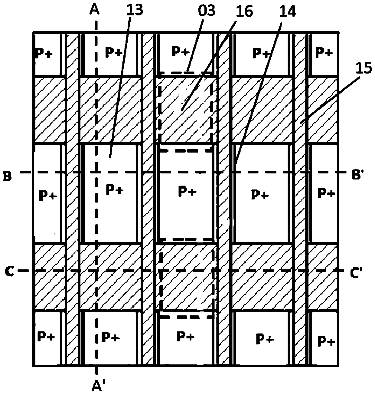
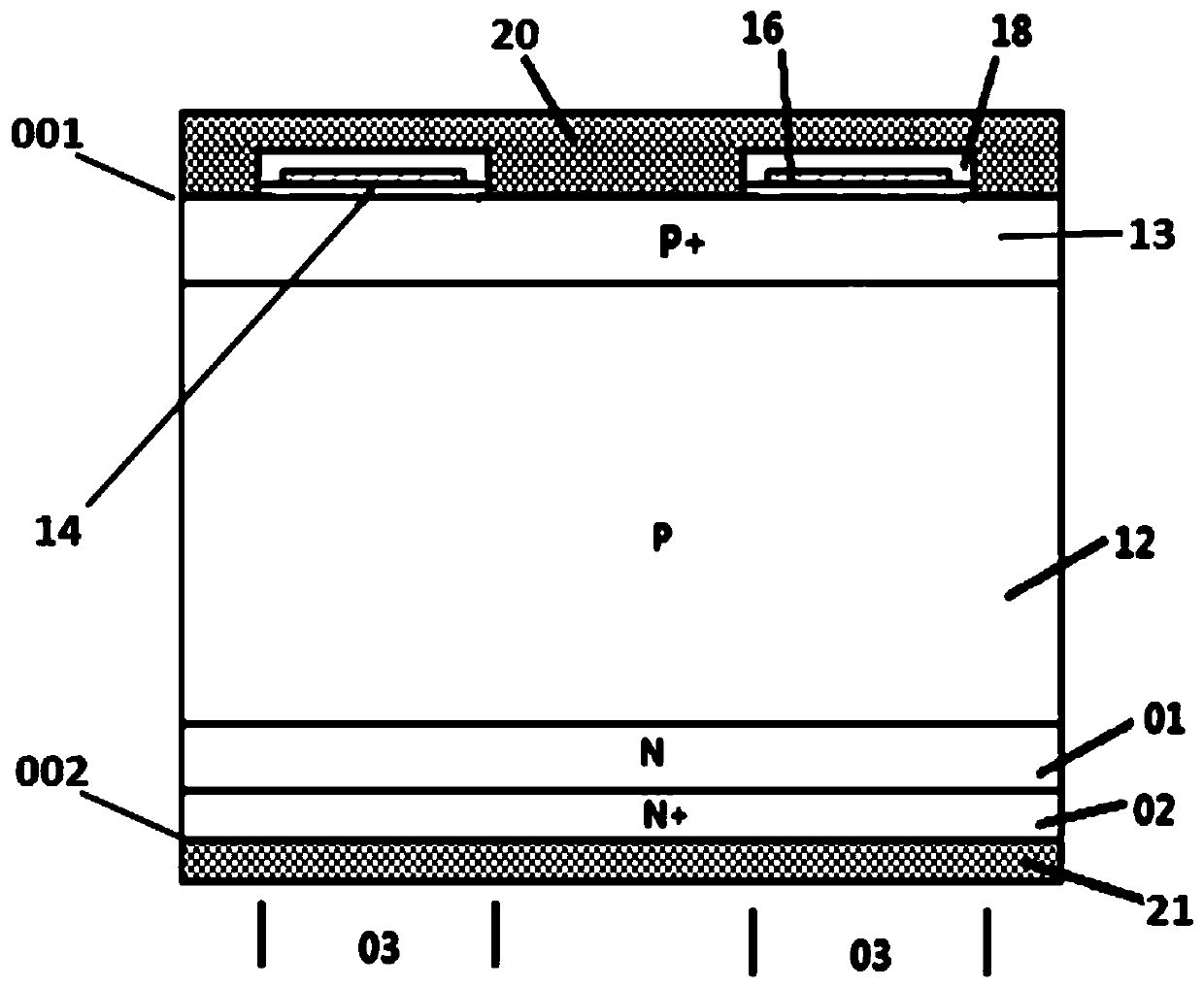
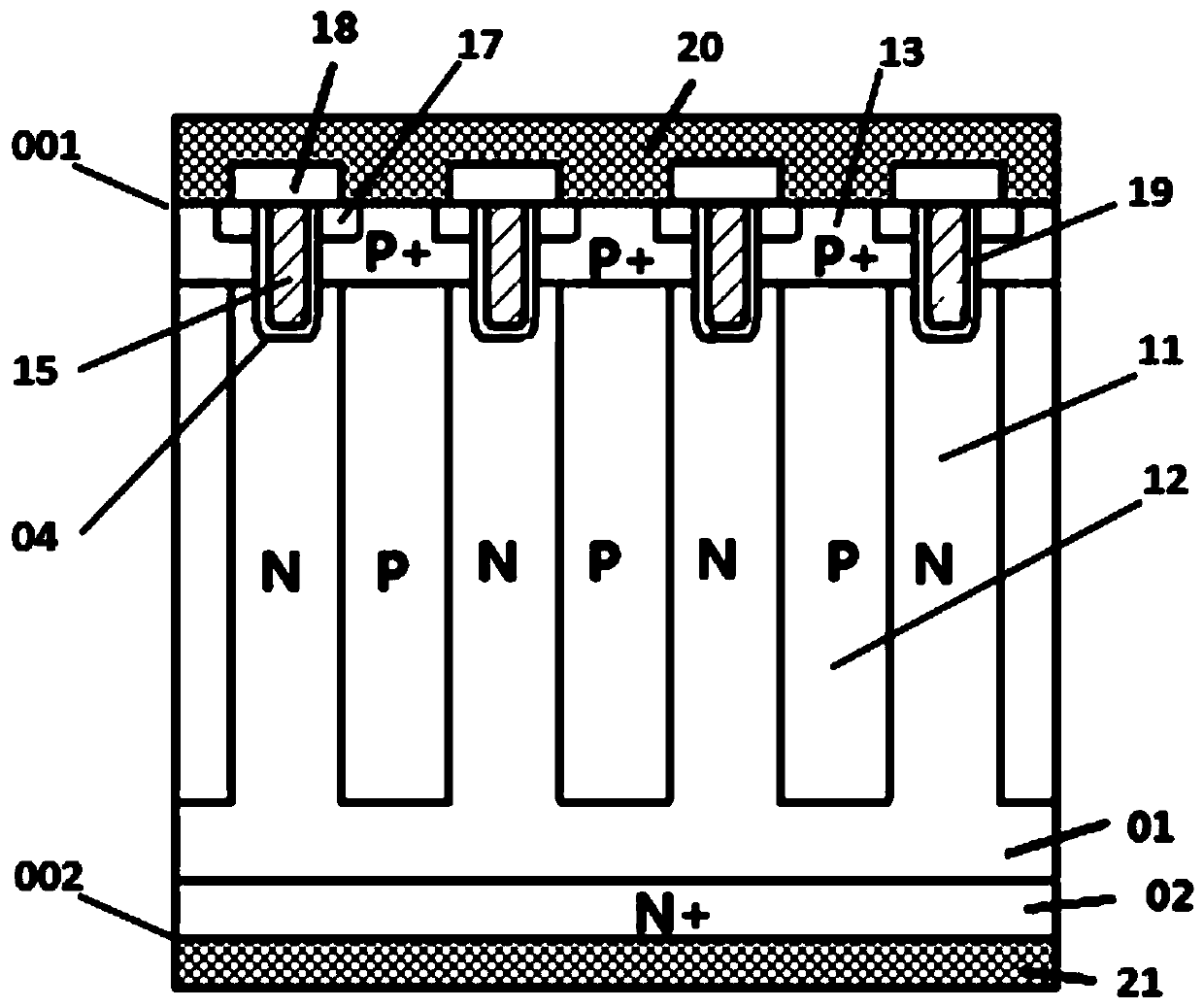
[0043] as attached figure 1 As shown in ~ 4, a super junction semiconductor device with optimized switching characteristics, taking an N-type trench gate super junction semiconductor device as an example, includes a cell area and a terminal protection area, the cell area is located in the central area of ​​the device, The terminal protection area surrounds the cell region, and the cell region includes a semiconductor substrate, and the semiconductor substrate includes a first conductivity type substrate 02 and a first conductivity type substrate 02 located on and adjacent to the first conductivity type substrate. A conductivity type drift region 01, the upper surface of the first conductivity type drift region 01 is the first main surface 001 of the semiconductor substrate, and the lower surface of the first conductivity type substrate 02 is the second main sur...


PUM


Abstract

The invention relates to a super junction semiconductor device with the optimized switching characteristic and a manufacturing method. The super junction semiconductor device is characterized that integrated capacitor areas are introduced into the surface of a trench gate type super junction semiconductor device, and each integrated capacitor comprises a gate capacitor plate, a first insulating medium layer and a second conduction type body area, wherein the areas, adjacent to a semiconductor substrate, of the first insulating medium layers in the section direction of the semiconductor are the second conduction type body areas, the first insulating medium layers are provided with the gate capacitor plates which are adjacent to one another, and the gate capacitor plates are electrically communicated with gate electrodes. According to the device, by introducing the integrated capacitor areas, the input capacitance Ciss of the device can be effectively increased, but the feeback capacitance Crss and the output capacitance Coss of the device are invariable, therefore, the ratio of the feedback capacitance Crss to the input capacitance Ciss is decreased, then the switching characteristic of the device is improved, and the ratio of dV to dt in the switching process is decreased; in addition, the manufacturing method of the device is compatible with an existing semiconductor technology, preparation of the integrated capacitor areas can be completed on the premise that no technological step is added, and therefore cost is not increased.

Description

technical field [0001] The invention relates to a super junction semiconductor device and a manufacturing method, in particular to a super junction semiconductor device and a manufacturing method with optimized switching characteristics. Background technique [0002] In the field of medium and high voltage power semiconductor devices, super junction structure (Super Junction) has been widely used. Compared with traditional power MOSFET devices, super junction structure MOSFET devices can obtain a better compromise relationship between device withstand voltage and on-resistance. The super junction structure is formed in the drift region of the semiconductor device. The super junction structure formed in the drift region includes N-conductivity type pillars (N pillars) and P conductivity-type pillars (P pillars). The N pillars and P pillars are alternately adjacent to each other. A plurality of P-N column pairs form a super junction structure. The N column has impurities of N...

Claims


Application Information

Patent Timeline
Patent Type & Authority Patents(China)
IPC IPC(8): H01L29/06H01L29/78H01L21/336
CPCH01L29/0634H01L29/66734H01L29/7803
Inventor 朱袁正李宗清
Owner WUXI NCE POWER
Why Eureka
Try Eureka