Method for reducing noise using layout scheme and comparing device

a comparing device and layout scheme technology, applied in the field of reducing horizontal noise of cmos image sensors, can solve the problems of difficult layout of interconnection lines for coupling passive elements, inability to accommodate passive elements, capacitors, etc., and achieve the effect of reducing horizontal noise in cmos image sensors

Active Publication Date: 2016-08-09
SK HYNIX INC
View PDF3 Cites 0 Cited by
  • Summary
  • Abstract
  • Description
  • Claims
  • Application Information

AI Technical Summary

Benefits of technology

[0007]Various embodiments of the present invention are directed to a method for reducing horizontal noise in CMOS image sensors using a layout scheme without using an additional capacitor, and a comparing device.
[0008]Various embodiments of the present invention are directed to a method for reducing horizontal noise of a CMOS image sensor using a layout scheme, and a comparing device by closely disposing an input line and an output line of a second stage comparator, increasing parasitic capacitance, inducing a Miller effect, increasing loading capacitance of an output line of a first stage comparator, reducing bandwidth of a comparing device, and reducing noise higher than a specific frequency inducing horizontal noise of the CMOS image sensor.
[0009]In accordance with an embodiment of the present invention, a method for reducing noise may include increasing parasitic capacitance by disposing an input line and an output line of a second stage comparator adjacent to each other, wherein the second stage comparator is disposed behind a first stage, which is coupled to the second stage comparator out of a plurality of stage comparators, increasing an input capacitance generated on the input line of the second stage comparator due to a Miller effect caused by an increased parasitic capacitance, and reducing noise having a frequency higher than a predetermined frequency through a reduction of bandwidth of a comparing device caused by an increased input capacitance.
[0010]In accordance with an embodiment of the present invention, a method for reducing a noise may include increasing a parasitic capacitance by disposing an input line and an output line of a second stage comparator adjacent to each other, wherein the second stage comparator is disposed behind a first stage comparator, which is coupled to the second stage comparator out of a plurality of stage comparators, increasing an input capacitance generated on the input line of the second stage comparator due to a Miller effect caused by an increased parasitic capacitance, and reducing a noise having a frequency higher than a predetermined frequency through a reduction of a bandwidth caused by an increased input capacitance.
[0011]In accordance with an embodiment of the present invention, a comparing device may include a first stage comparator, and a second stage comparator disposed behind the first stage comparator coupled to the second stage comparator, wherein a parasitic capacitance is increased by disposing an input line and an output line of the second stage comparator adjacent to each other, an input capacitance generated on the input line of the second stage comparator due to a Miller effect caused by an increased parasitic capacitance is increased, and a noise having a frequency higher than a predetermined frequency through a reduction of a bandwidth of a comparing device caused by an increased input capacitance is reduced.

Problems solved by technology

If the pitch is too small, passive elements (e.g., a capacitor) may not be able to be accommodated because the size of the passive element may be larger than the pixel pitch and the layout of interconnection lines for coupling the passive elements may be difficult.

Method used


Image

  • Method for reducing noise using layout scheme and comparing device
  • Method for reducing noise using layout scheme and comparing device
  • Method for reducing noise using layout scheme and comparing device

Examples


Embodiment Construction

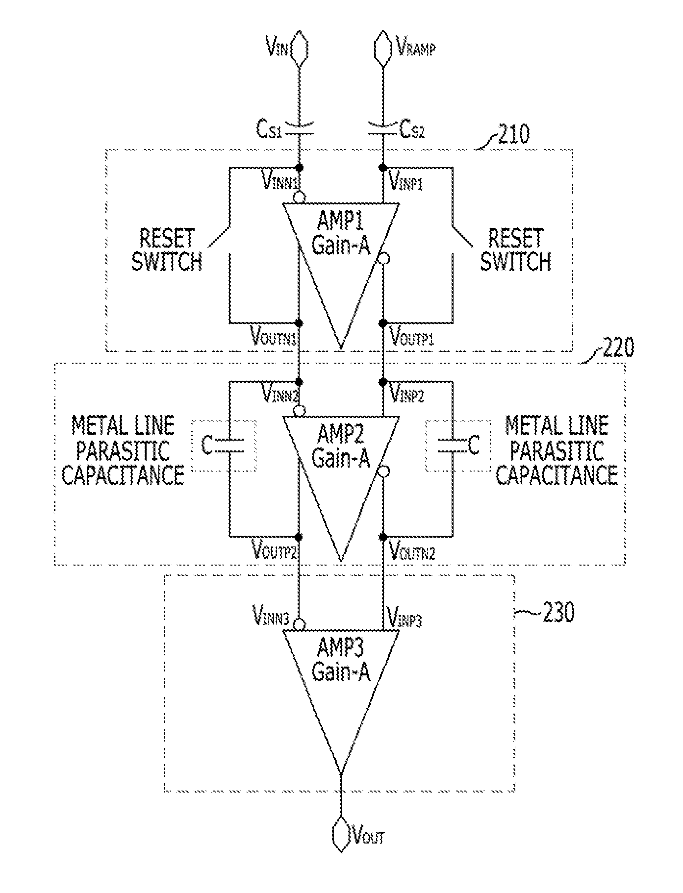
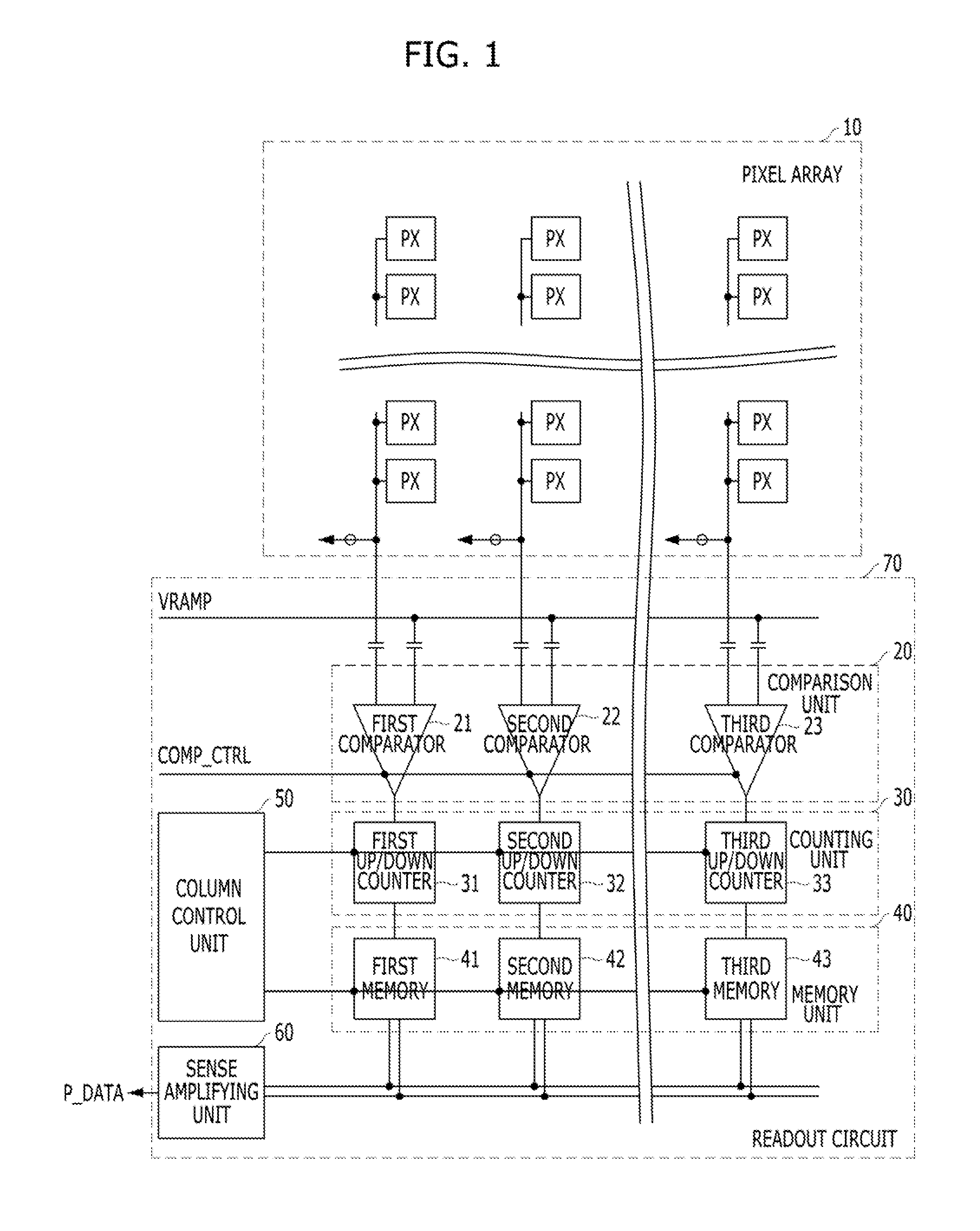
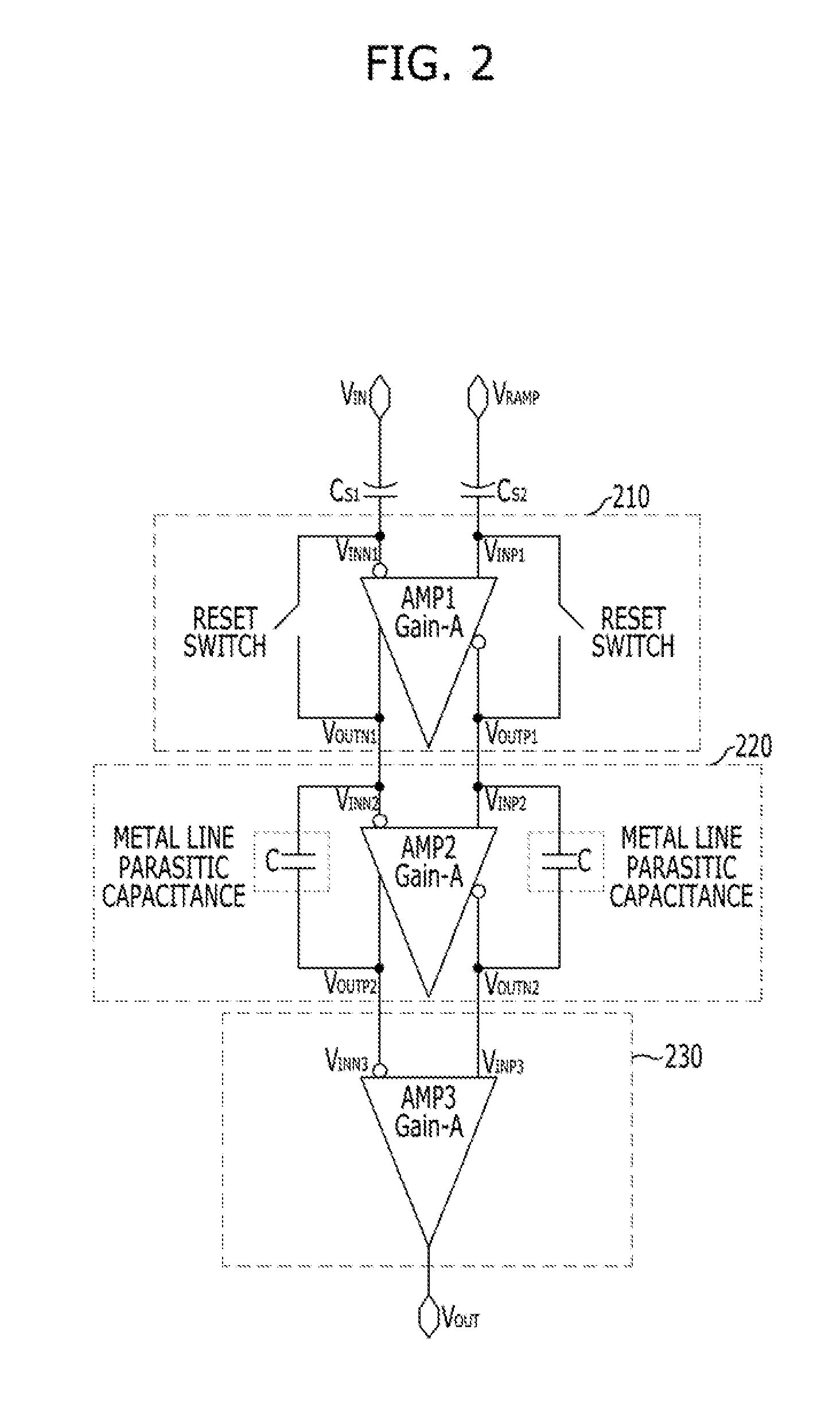
[0017]Exemplary embodiments of the present invention will be described below in more detail with reference to the accompanying drawings. The present invention may however, be embodied in different forms and should not be construed as limited to the embodiments set forth herein. Rather, these embodiments are provided so that this disclosure will be thorough and complete, and will fully convey the scope of the present invention to those skilled in the art. Throughout the disclosure, reference numerals correspond directly to the like parts in the various figures and embodiments of the present invention.

[0018]The drawings are not necessarily to scale and, in some instances, proportions may have been exaggerated in order to clearly illustrate features of the embodiments. In this specification, specific terms have been used. The terms are used to describe the present invention and are not used to qualify the sense or limit the scope of the present invention.

[0019]It is also noted that in ...


PUM


Abstract

A comparing device includes a first stage comparator and a second stage comparator serially coupled to the first stage comparator, wherein output lines of the second stage comparator are disposed to be overlapped with respective input lines of the second stage comparator.

Description

CROSS-REFERENCE TO RELATED APPLICATIONS[0001]The present application claims priority of Korean Patent Application No. 10-2014-0033465, filed on Mar. 21, 2014, which is incorporated herein by reference in its entirety.BACKGROUND[0002]1. Field[0003]Various embodiments of the present invention relate to a complementary metal oxide semiconductor (CMOS) image sensor and, more particularly, to a method for reducing horizontal noise of the CMOS image sensor using a layout scheme and a comparing device.[0004]2. Description of the Related Art[0005]In CMOS image sensors using single-slope analog-to-digital converters, data is distorted by various noises. Noise may occur in both the pixel signals (outputted from the pixel array) and the ramp signal (outputted from a ramp signal generation device) when the data of each row of pixels is processed. This noise is called horizontal noise.[0006]As the number of pixels in the CMOS image sensor increases, the pitch of the pixels is reduced. If the pit...

Claims


Application Information

Patent Timeline
Patent Type & Authority Patents(United States)
IPC IPC(8): H03K5/1252H03K5/24
CPCH03K5/1252H03K5/24
Inventor YOO, SI-WOOK
Owner SK HYNIX INC
Why Eureka
Try Eureka