Liquid crystal display device and electronic apparatus

a liquid crystal display and electronic device technology, applied in non-linear optics, instruments, optics, etc., can solve the problems of brightness deterioration, difficult to twist liquid crystal molecules on the electrodes or between the electrodes, etc., to achieve high-quality display

Inactive Publication Date: 2010-04-15
JAPAN DISPLAY INC
View PDF9 Cites 57 Cited by
  • Summary
  • Abstract
  • Description
  • Claims
  • Application Information

AI Technical Summary

Benefits of technology

[0046]By including the liquid crystal display device in the display unit, it is possible to realize high-quality display in the display unit.

Problems solved by technology

However, in the IPS mode liquid crystal display device 150, it is difficult to twist liquid crystal molecules on the electrodes by the size of the electric field strength such that brightness of display deteriorates.
In the FFS mode liquid crystal display device 190, it is difficult to twist liquid crystal molecules on the electrodes or between the electrodes by the size of the electric field strength such that brightness of display deteriorates.

Method used


Image

  • Liquid crystal display device and electronic apparatus
  • Liquid crystal display device and electronic apparatus
  • Liquid crystal display device and electronic apparatus

Examples


first embodiment

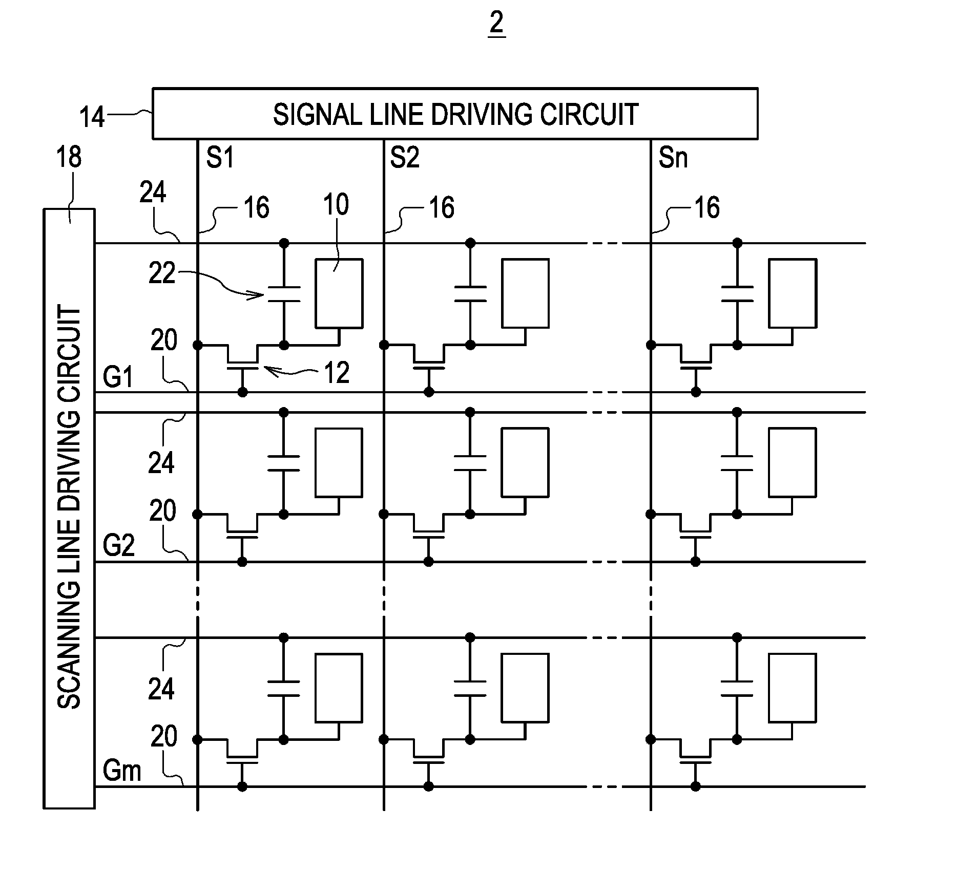
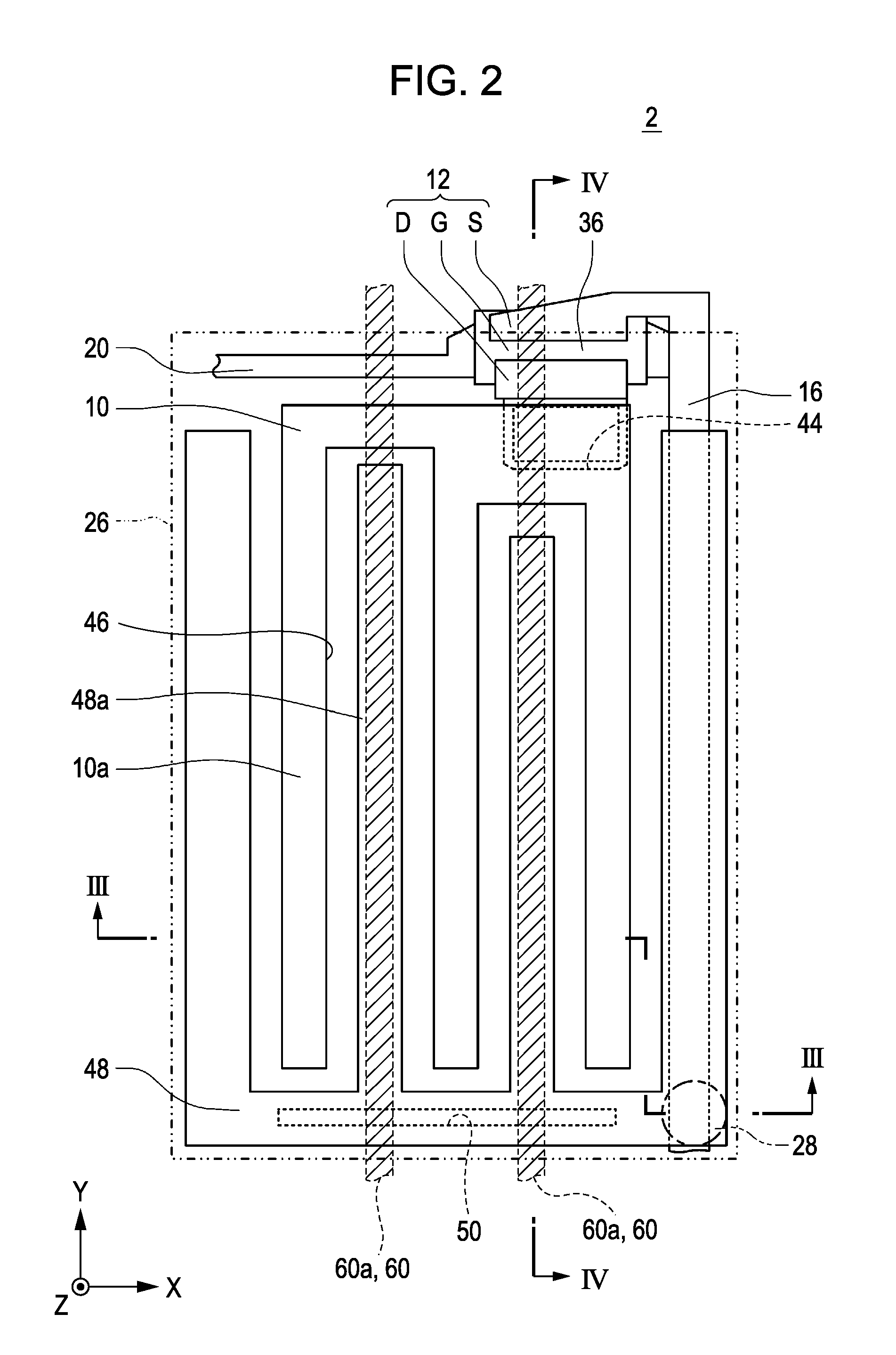
[0075]FIG. 1 is a circuit diagram of a plurality of sub pixel regions formed in a matrix configuring a liquid crystal display device 2 according to the present embodiment.

[0076]In an image display region of the liquid crystal display device 2 according to the present embodiment, a plurality of sub pixels regions is arranged in a matrix. In each of the sub pixel regions, a first electrode 10 and a TFT 12 for controlling switching of the first electrode 10 are formed. Each of signal lines 16 extending from a signal line driving circuit 14 is electrically connected to a source of the TFT 12. The signal line driving circuit 14 supplies image signals S1, S2, . . . , and Sn to pixels via the signal lines 16. The image signals S1 to Sn may be line-sequentially supplied in this order or may be supplied to a group of a plurality of adjacent signal lines 16.

[0077]Each of scanning lines 20 extending from a scanning line driving circuit 18 is electrically connected to a gate of the TFT 12. The ...

second embodiment

[0100]Next, a liquid crystal display device 4 according to a second embodiment will be described with reference to FIGS. 6 to 8.

[0101]FIG. 6 is a plan view of any one sub pixel seen through a color filter substrate CF of the liquid crystal display device 4 according to the present embodiment. FIG. 7 is a partial cross-sectional view taken along line VII-VII of FIG. 6. FIG. 8 is a partial cross-sectional view taken along line VIII-VIII of FIG. 6. In addition, in FIGS. 6 to 8, the same components as the liquid crystal display device 2 of the first embodiment shown in FIGS. 2 to 4 are denoted by the same reference numerals and the detailed description thereof will be omitted.

[0102]The liquid crystal display device 4 according to the present embodiment is different from the liquid crystal display device 2 according to the first embodiment in that fourth and fifth electrodes 70 and 72 of lower electrodes are formed in addition to the first and second electrodes 10 and 48 on the side of t...

third embodiment

[0117]Next, a liquid crystal display device 6 according to a third embodiment will be described with reference to FIG. 10.

[0118]FIG. 10 is a plan view of any one sub pixel seen through a color filter substrate CF of the liquid crystal display device 6 according to the present embodiment. In FIG. 10, the same components as the liquid crystal display device 4 of the second embodiment shown in FIG. 6 are denoted by the same reference numerals and the detailed description thereof will be omitted. The cross-sectional views of FIG. 10 corresponding to line VII-VII and VIII-VIII of FIG. 6 are equal to FIGS. 7 and 8 and thus showing and detailed description thereof will be omitted.

[0119]The liquid crystal display device 6 according to the present embodiment is different from the liquid crystal display device 4 according to the second embodiment in that, whereas the linear portions 10a of the first electrode 10 and the linear portions 48a of the second electrode 48 straightly extend along th...


PUM

PropertyMeasurementUnit
electric fieldsaaaaaaaaaa
transparentaaaaaaaaaa
voltageaaaaaaaaaa

Abstract

Provided is a liquid crystal display device including: first and second substrates with a liquid crystal layer interposed therebetween; a first electrode formed on the liquid crystal layer side of the first substrate and having linear portions; a second electrode having linear portions formed along the linear portions of the first electrode and adjacent to the linear portions of the first electrode at a gap in plan view; and a third electrode formed on the liquid crystal layer side of the second substrate and having linear portions overlapping with the linear portions of the second electrode in plan view, wherein electric fields having different directions are generated between the first electrode and the second electrode and between the first electrode and the third electrode.

Description

BACKGROUND[0001]1. Technical Field[0002]The present invention relates to a liquid crystal display device and an electronic apparatus.[0003]2. Related Art[0004]As a liquid crystal display device, a vertical electric field mode liquid crystal display device such as a Twisted Nematic (TN) mode, a Vertical Alignment (VA) mode or a Multi-domain Vertical Alignment (MVA) mode is widely used, but a lateral electric field mode liquid crystal display device including electrodes on one substrate is also known. In the lateral electric field mode liquid crystal display device, the operation principle of an In-Plane Switching (IPS) mode liquid crystal display device will be described with reference to FIGS. 22 and 23 (for example, see JP-A-2003-140188).[0005]FIG. 22 is a schematic plan view of one pixel seen through a color filter substrate CF of a known IPS mode liquid crystal display device 150. FIG. 23 is a cross-sectional view taken along line XXIII-XXIII of FIG. 22.[0006]This IPS mode liquid...

Claims


Application Information

Patent Timeline
Patent Type & Authority Applications(United States)
IPC IPC(8): G02F1/1343
CPCG02F1/134363G02F2001/133397G02F2201/40G02F2001/134372G02F2001/134381G02F2001/134345G02F1/133397G02F1/134345G02F1/134372G02F1/134381G02F1/13439
Inventor NISHIMURA, JOJIYATA, TATSUYAKURASAWA, HAYATO
Owner JAPAN DISPLAY INC
Why Eureka
Try Eureka