Stacked thin-film superlattice thermoelectric devices
- Summary
- Abstract
- Description
- Claims
- Application Information
AI Technical Summary
Benefits of technology
Problems solved by technology
Method used
Image

Examples
Example
MODE(S) OF IMPLEMENTATION
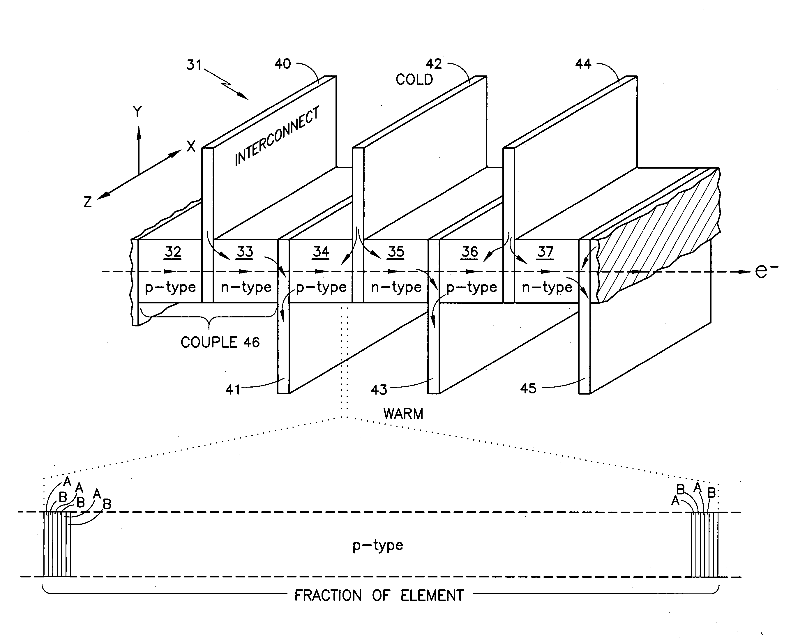
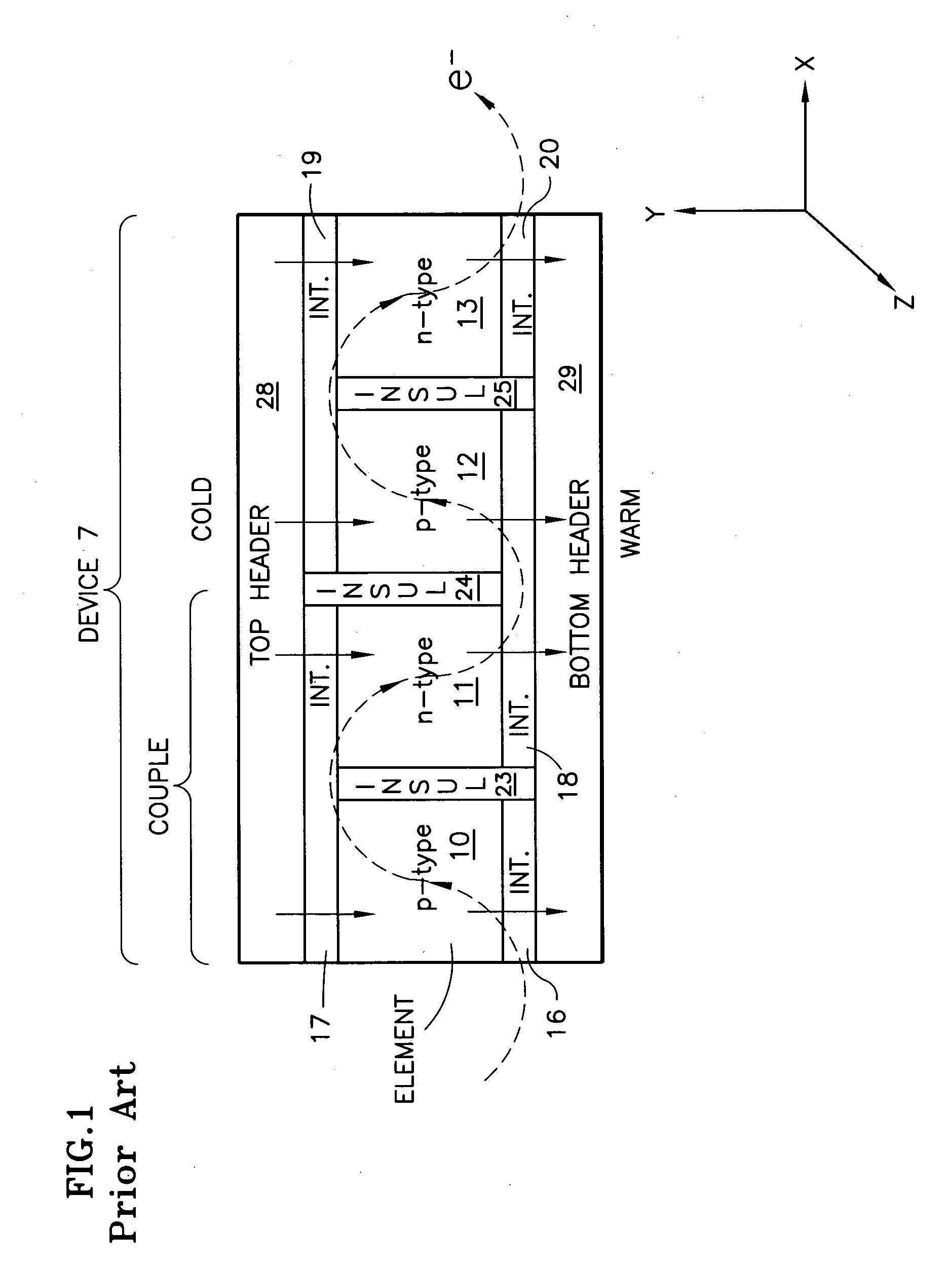
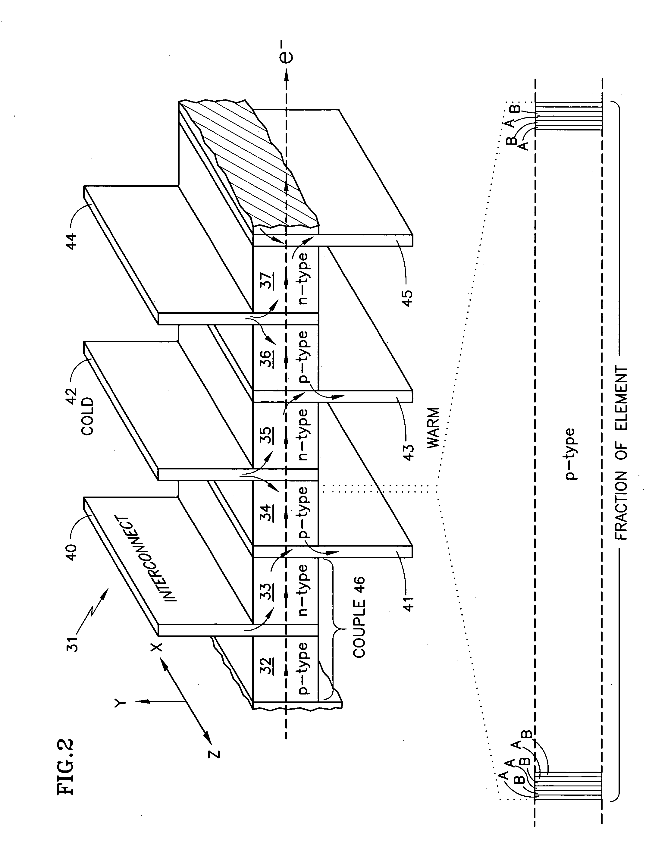
[0023]Referring to FIG. 1, a conventional thermoelectric device 7 includes a plurality of elements 10-13 each comprising a single thermoelectric alloy. The elements 10-13 are traditionally formed of Group V-VI semiconductor elements from the Bi2Te3—Sb2Te3—Bi2Se3 ternary system of materials. The alloy of the p-type elements 10, 12 may comprise, for instance, a ternary alloy of antimony, bismuth and tellurium, such as Sb1.5 Bi0.5 Te3.0. The alloy of the n-type elements 11, 13 may comprise a ternary alloy of bismuth, tellurium and selenium, such as Bi2 Te2.7 Se3.0. The bulk-material elements 10-13 may typically be approximately cubic in shape (not to be confused with cubic crystal structure), with between about 0.1 mm and 1.0 mm in each of the X, Y and Z directions.
[0024]The elements 10-13 are serially connected through interconnects (INT) 16-20. The upper interconnects 17, 19 are thermally and electrically insulated from the lower interconnects 16, 18 and 20 ...
PUM
 Abstract
Description
Claims
Application Information
 - Generate Ideas
- Intellectual Property
- Life Sciences
- Materials
- Tech Scout
- Unparalleled Data Quality
- Higher Quality Content
- 60% Fewer Hallucinations
Browse by: Latest US Patents, China's latest patents, Technical Efficacy Thesaurus, Application Domain, Technology Topic, Popular Technical Reports.
© 2025 PatSnap. All rights reserved.Legal|Privacy policy|Modern Slavery Act Transparency Statement|Sitemap|About US| Contact US: help@patsnap.com