

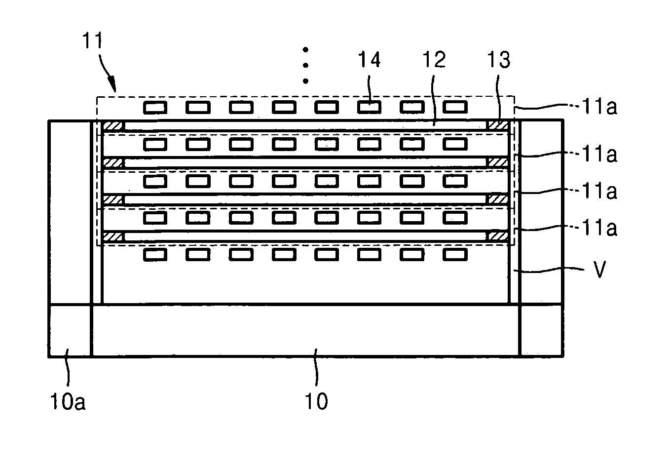
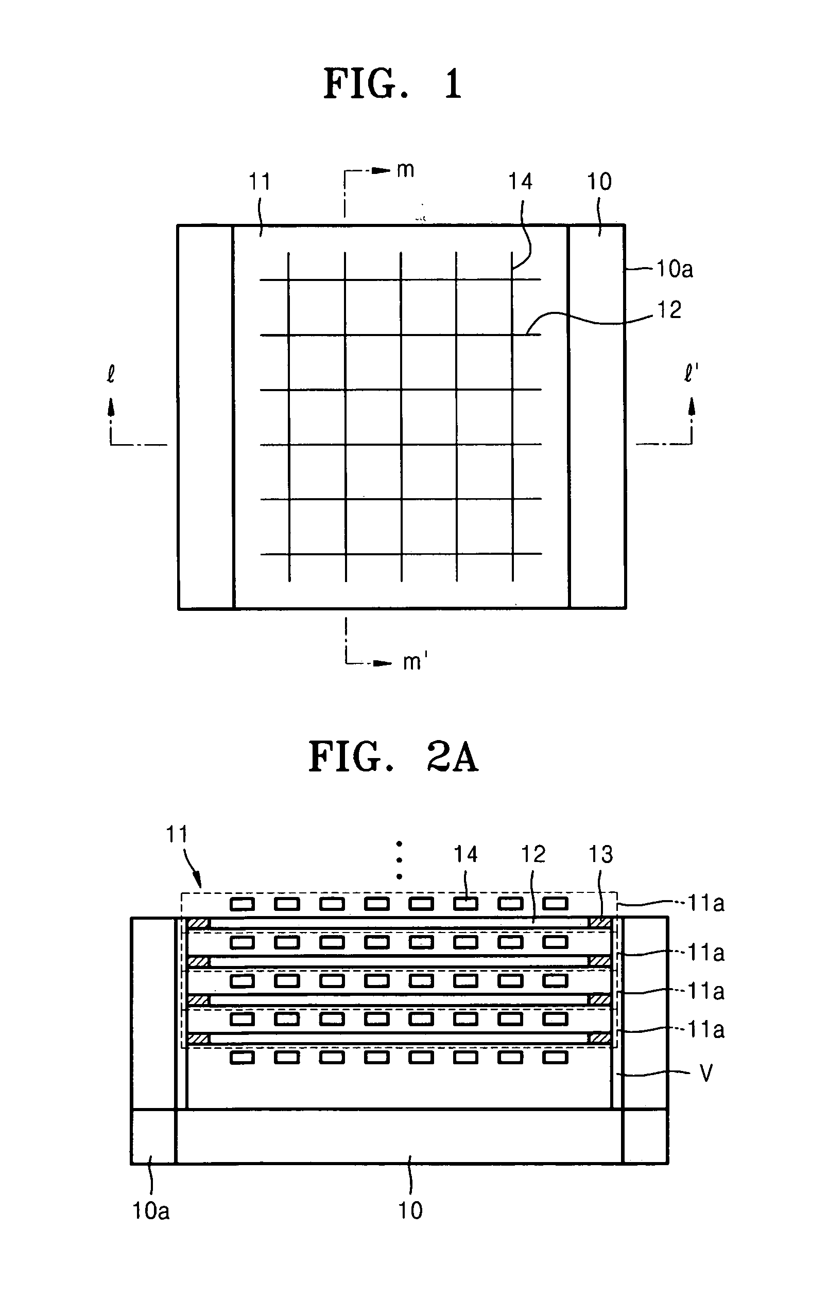
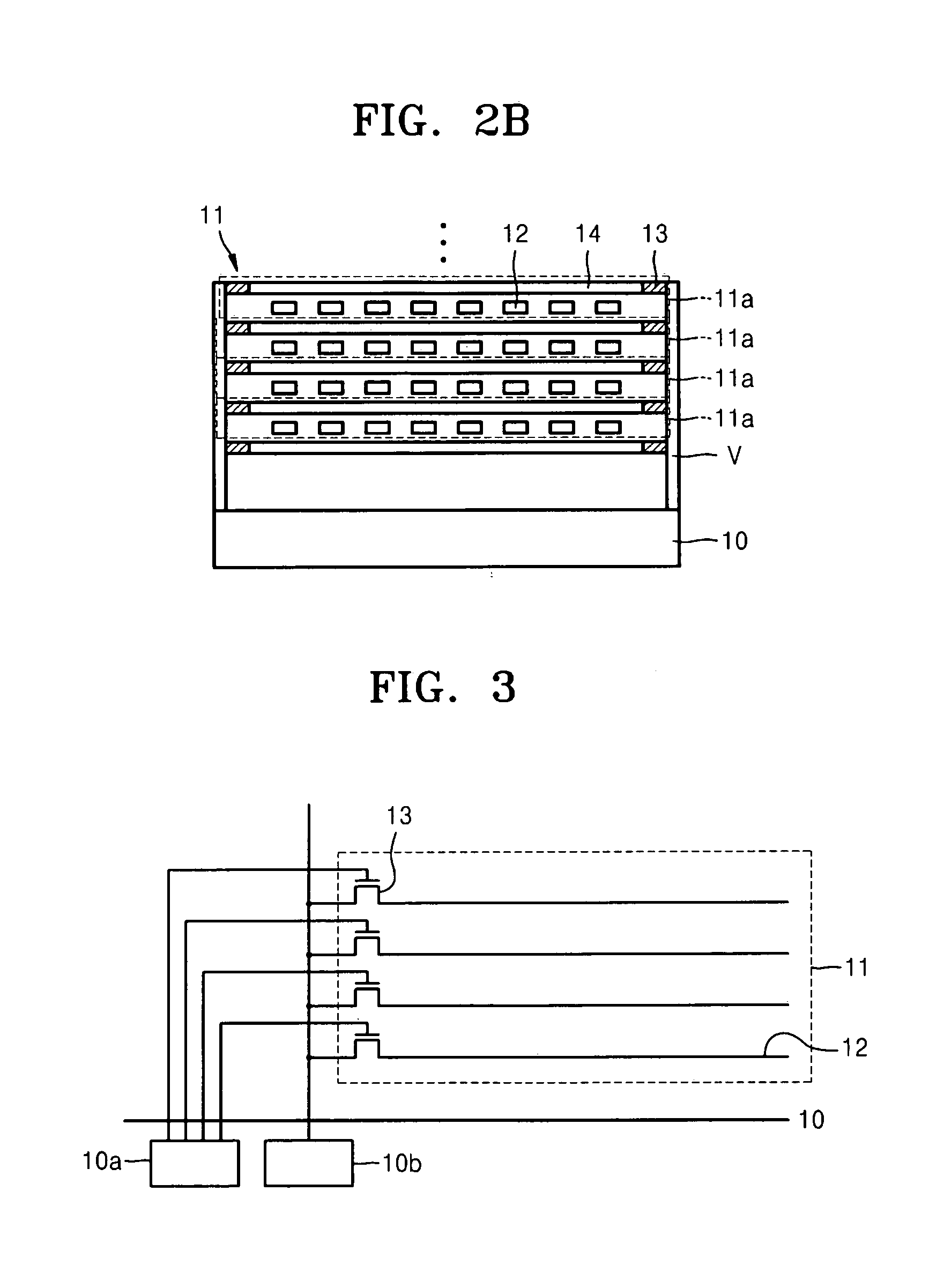
Multi-layered memory apparatus including oxide thin film transistor
a technology of oxide thin film transistors and memory devices, applied in transistors, optics, instruments, etc., can solve the problem of excessive increase in active circuit unit size, and achieve the effect of minimizing the size of active circuit uni
- Summary
- Abstract
- Description
- Claims
- Application Information
AI Technical Summary
Benefits of technology
Problems solved by technology
Method used
Image

Examples
Embodiment Construction
[0033]Example embodiments will be more clearly understood from the detailed description taken in conjunction with the accompanying drawings.
[0034]Various example embodiments will now be described more fully with reference to the accompanying drawings in which some example embodiments are shown. In the drawings, the thicknesses of layers and regions may be exaggerated for clarity.
[0035]Detailed illustrative example embodiments are disclosed herein. However, specific structural and functional details disclosed herein are merely representative for purposes of describing example embodiments. Other embodiments may, however, may be embodied in many alternate forms and should not be construed as limited to only the example embodiments set forth herein.
[0036]Accordingly, while example embodiments are capable of various modifications and alternative forms, example embodiments thereof are shown by way of example in the drawings and will herein be described in detail. It should be understood, ...
PUM
 Abstract
Description
Claims
Application Information