Image display device

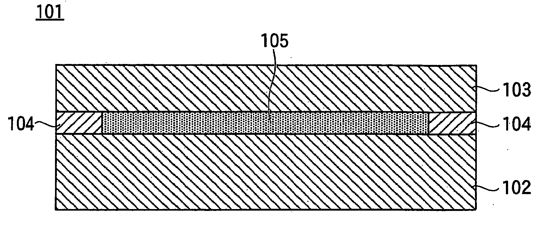
a display device and image technology, applied in the direction of identification means, electrical apparatus casings/cabinets/drawers, instruments, etc., can solve the problems of display defects, deformation of optical glass, and gap 105, and achieve the effect of suppressing the influence of stress

Active Publication Date: 2010-04-22
DEXERIALS CORP
View PDF30 Cites 47 Cited by
  • Summary
  • Abstract
  • Description
  • Claims
  • Application Information

AI Technical Summary

Benefits of technology

[0016]Generally, the assembly of an image display device requires a certain gap between the image display unit and the frame member surrounding the image display unit, and the backlight appears on the bottom of the gap. In the image display device of the invention and the method of manufacturing the same, a photo-curable resin composition is interposed between the protecting member and the display-side panel into which the image display unit and the frame member are incorporated. Then, the photo-curable resin composition is photo-cured. In this photo-curing process, a photo-curable resin composition having a particular viscosity is used, or the gap between the image display unit and the frame member is covered with a sealing film. Therefore, the photo-curable resin composition is prevented from entering the gap between the image display unit and the frame member and flowing toward the backlight.
[0017]In this instance, a resin composition having a curing shrinkage ratio of 5% or less and forming a photo-cured resin layer having a light transmittance of 90% or more in a visible region and a storage elastic modulus at 25° C. of 1.0×10⁷ Pa or less is used as the photo-curable resin composition. The use of such a resin composition can suppress the influence of the stress during curing and shrinkage of the resin on the image display unit and the protection member as much as possible. Therefore, advantageously, almost no strain occurs in the image display unit and the protection member. In addition, the size of the gap between the image display unit and the frame member do not change.
[0018]Therefore, in the present invention, the above advantageous effects work synergistically and allow high-brightness and high-contrast display without display defects.

Problems solved by technology

The presence of the gap 105 is an obstacle to the reduction in thickness of the panel.
However, the stress during the cure shrinkage of the cured resin causes deformation of the optical glass plates sandwiching the liquid crystal of the liquid crystal display panel.
This results in display defects such as irregularities in orientation of the liquid crystal material.
Unfortunately, when the gap between the liquid crystal display panel and the protection member is filled with the resin composition, the resin composition may adhere to the backlight side under some manufacturing conditions.

Method used


Image

  • Image display device
  • Image display device
  • Image display device

Examples


first embodiment

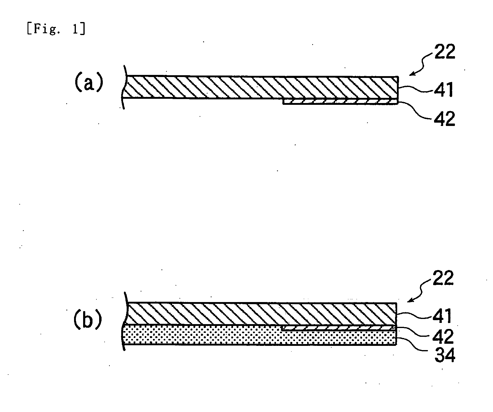
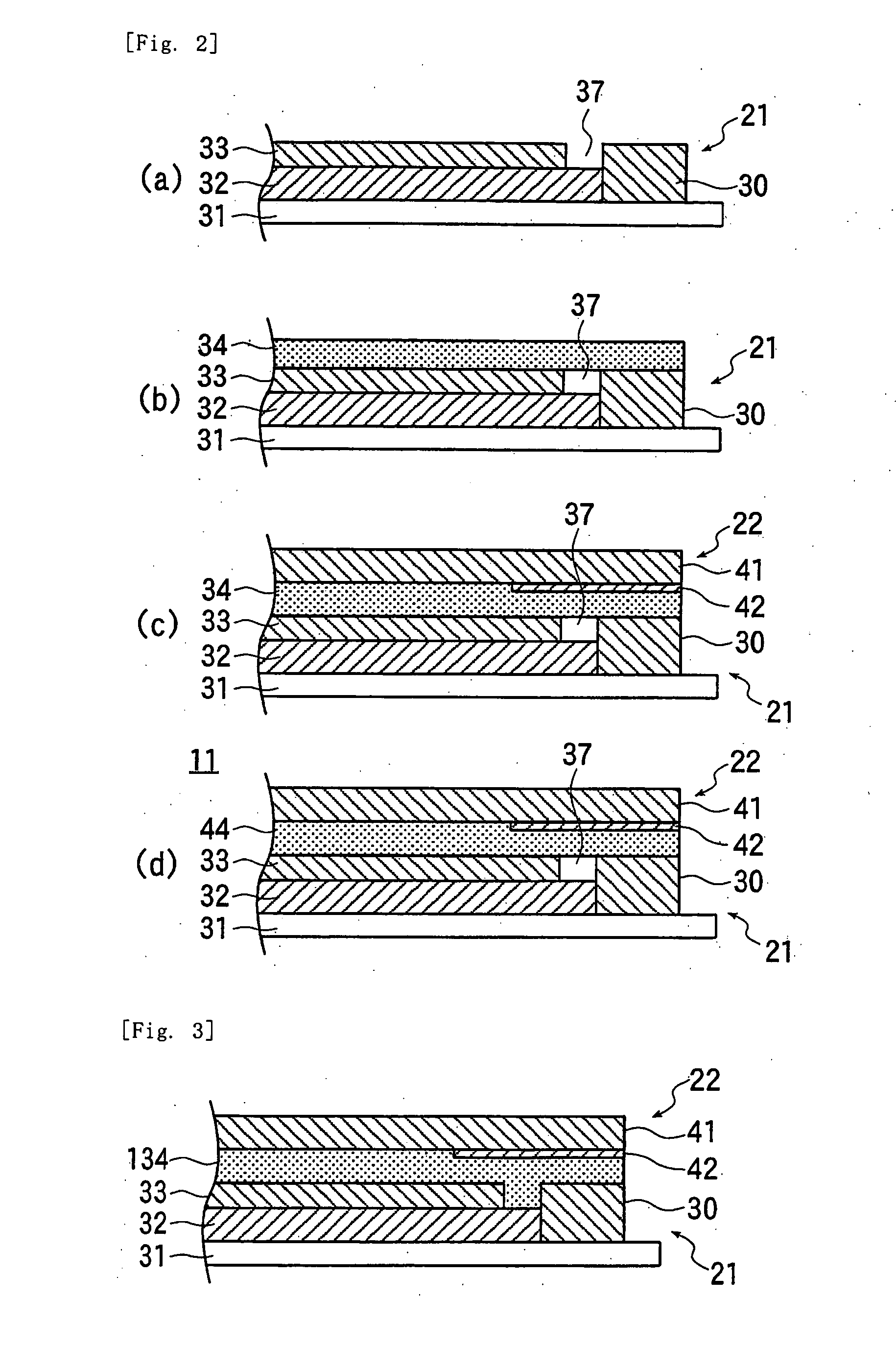
[0039]FIG. 2 is a series of cross-sectional views illustrating the main part of a method for manufacturing an image display device 11 (FIG. 2(d)) according to a first embodiment of the present invention. In this image display device 11, a protection member 22 is bonded to a display-side panel 21 through a cured resin layer 44.

[0040]A description is given of the manufacturing process of the image display device 11. As shown in FIG. 2(a), in the display-side panel 21 before bonding through the cured resin layer 44, a frame member 30 surrounding an image display unit is disposed on a plate-like base 31, and a backlight 32 and the image display unit 33 including a liquid crystal panel smaller than the backlight 32 are disposed in that order on the base 31 so as to be located inside the frame member 30. The frame member 30 may be integrated with the base 31.

[0041]In this state, a gap 37 having a maximum width of several mm is formed between the image display unit 33 and the frame member ...

second embodiment

[0051]FIG. 4 is a cross-sectional view illustrating the main part of a method for manufacturing an image display device 12 of a second embodiment.

[0052]In the method for manufacturing in the second embodiment, a resin composition having a low viscosity (less than 3000 mPa·s) is used as a photo-curable resin composition. If applied to the display-side panel 21 in the same manner as in the first embodiment, the photo-curable resin composition 134 flows into the gap 37, as shown in FIG. 3. When the photo-curable resin composition 134 flows into the gap 37 as shown in FIG. 3, the resin composition 134 may penetrate between the backlight 32 and the image display unit 33. This may cause display defects.

[0053]Therefore, in the second embodiment, before the photo-curable resin composition is applied to the display-side panel 21, an adhesive sealing film 51 is disposed so as to cover the gap 37 of the display-side panel 21 in the state shown in FIG. 2(a). More specifically, the sealing film ...

third embodiment

[0058]FIG. 5 is a series of cross-sectional views illustrating the main part of a method for manufacturing an image display device 13 of a third embodiment.

[0059]The manufacturing method in the third embodiment is different from the manufacturing method in the second embodiment in that a display-side panel 24 including a frame member 61 having a protruding portion 62 on its side circumferential edges is used as shown in FIG. 5(a).

[0060]Also in this display-side panel 24, a gap 57 is formed between the frame member 61 and the image display unit 33, and the backlight 32 appears on the bottom of the gap 57.

[0061]First, as, shown in FIG. 5(b), the sealing film 51 is applied so as to cover the gap 57. More specifically, the sealing film 51 is applied so as to be disposed across between the image display unit 33 and the frame member 61, whereby the gap 57 is sealed.

[0062]Next, as shown in FIG. 5(c), a photo-curable resin composition 36 is applied dropwise to the display-side panel 24 so a...


PUM

PropertyMeasurementUnit
viscosityaaaaaaaaaa
viscosityaaaaaaaaaa
light transmittanceaaaaaaaaaa

Abstract

A method for manufacturing an image display device includes the step of forming a cured resin layer by interposing a photo-curable resin composition between a protection member and a display-side panel including an image display unit and a frame member and then photo-curing the photo-curable resin composition, with the photo-curable resin composition being disposed across between the image display unit and the frame member. In the manufacturing method, a high-viscosity resin composition having a viscosity of 3000 mPa·s or more and 12000 mPa·s or less is used as the photo-curable resin composition. Alternatively, after a gap between the image display unit and the frame member is sealed with a sealing film, a photo-curable resin composition is interposed between the display-side panel and the protection member.

Description

TECHNICAL FIELD[0001]The present invention relates to an image display device such as a liquid crystal display (LCD) device used, for example, in a cellular phone, and in particular, to an image display device having a transparent protection member disposed on an image display unit and a method for manufacturing the same.BACKGROUND TECHNOLOGY[0002]One conventional example of such a display device is a liquid crystal display device 101 shown in FIG. 6. This liquid crystal display device 101 includes a transparent protection member 103 made of, for example, glass or plastic and disposed on a liquid crystal display panel 102.[0003]In this case, to protect the surface of the liquid crystal display panel 102 and a polarizing plate (not shown), a spacer 104 is interposed between the liquid crystal display panel 102 and the protection member 103, so that a gap 105 is provided between the liquid crystal display panel 102 and the protection member 103.[0004]However, the gap 105 present betwe...

Claims


Application Information

Patent Timeline
Patent Type & Authority Applications(United States)
IPC IPC(8): H05K5/00H01J9/00
CPCG02F1/133308G02F2001/133311G02F2201/086G02B1/105G02F2202/023G02F2202/28G02F2201/50G02B1/10G02F1/133311G02B1/11G09F9/35G02F1/133331G02B1/14
Inventor TOYODA, TOMOYUKISHINYA, YOSHIHISAKAMATA, YUSUKE
Owner DEXERIALS CORP
Why Eureka
Try Eureka